
Calculator User Manual
Table Of Contents
- Read This First
- Contents
- Figures
- Tables
- Examples
- Cautions
- Introduction
- Architectural Overview
- Central Processing Unit
- Memory and I/O Spaces
- Program Control
- Addressing Modes
- Assembly Language Instructions
- Instruction Set Summary
- How To Use the Instruction Descriptions
- Instruction Descriptions
- ABS
- ABS
- ADD
- ADD
- ADD
- ADD
- ADDC
- ADDC
- ADDS
- ADDS
- ADDT
- ADDT
- ADRK
- AND
- AND
- AND
- APAC
- APAC
- B
- BACC
- BANZ
- BANZ
- BCND
- BCND
- BIT
- BIT
- BITT
- BITT
- BLDD
- BLDD
- BLDD
- BLDD
- BLDD
- BLPD
- BLPD
- BLPD
- BLPD
- CALA
- CALL
- CC
- CC
- CLRC
- CLRC
- CMPL
- CMPR
- DMOV
- DMOV
- IDLE
- IN
- IN
- INTR
- LACC
- LACC
- LACC
- LACL
- LACL
- LACL
- LACT
- LACT
- LAR
- LAR
- LAR
- LDP
- LDP
- LPH
- LPH
- LST
- LST
- LST
- LST
- LT
- LT
- LTA
- LTA
- LTD
- LTD
- LTD
- LTP
- LTP
- LTS
- LTS
- MAC
- MAC
- MAC
- MAC
- MACD
- MACD
- MACD
- MACD
- MACD
- MAR
- MAR
- MPY
- MPY
- MPY
- MPYA
- MPYA
- MPYS
- MPYS
- MPYU
- MPYU
- NEG
- NEG
- NMI
- NOP
- NORM
- NORM
- NORM
- OR
- OR
- OR
- OUT
- OUT
- PAC
- POP
- POP
- POPD
- POPD
- PSHD
- PSHD
- PUSH
- RET
- RETC
- ROL
- ROR
- RPT
- RPT
- SACH
- SACH
- SACL
- SACL
- SAR
- SAR
- SBRK
- SETC
- SETC
- SFL
- SFR
- SFR
- SPAC
- SPH
- SPH
- SPL
- SPL
- SPLK
- SPLK
- SPM
- SQRA
- SQRA
- SQRS
- SQRS
- SST
- SST
- SUB
- SUB
- SUB
- SUB
- SUBB
- SUBB
- SUBC
- SUBC
- SUBS
- SUBS
- SUBT
- SUBT
- TBLR
- TBLR
- TBLR
- TBLW
- TBLW
- TBLW
- TRAP
- XOR
- XOR
- XOR
- ZALR
- ZALR
- On-Chip Peripherals
- Synchronous Serial Port
- Asynchronous Serial Port
- TMS320C209
- Register Summary
- TMS320C1x/C2x/C2xx/C5x Instruction Set Comparison
- Program Examples
- Submitting ROM Codes to TI
- Design Considerations for Using XDS510 Emulator
- E.1 Designing Your Target System’s Emulator Connector (14-Pin Header)
- E.2 Bus Protocol
- E.3 Emulator Cable Pod
- E.4 Emulator Cable Pod Signal Timing
- E.5 Emulation Timing Calculations
- E.6 Connections Between the Emulator and the Target System
- E.7 Physical Dimensions for the 14-Pin Emulator Connector
- E.8 Emulation Design Considerations
- Glossary
- Index
Input Scaling Section
3-4
Shift count. The shifter can left-shift a 16-bit value by 0 to 16 bits. The size
of the shift (or the shift count) is obtained from one of two sources:
A constant embedded in the instruction word.
Putting the shift count in the
instruction word allows you to use specific data-scaling or alignment op-
erations customized for your program code.
The four LSBs of the temporary register (TREG).
The TREG-based shift
allows the data-scaling factor to be determined dynamically so that it can
be adapted to the system’s performance.
Sign-extension mode bit. For many but not all instructions, the sign-exten-
sion mode bit (SXM), bit 10 of status register ST1, determines whether the
CALU uses sign extension during its calculations. If SXM = 0, sign extension
is suppressed. If SXM = 1, the output of the input shifter is sign extended.
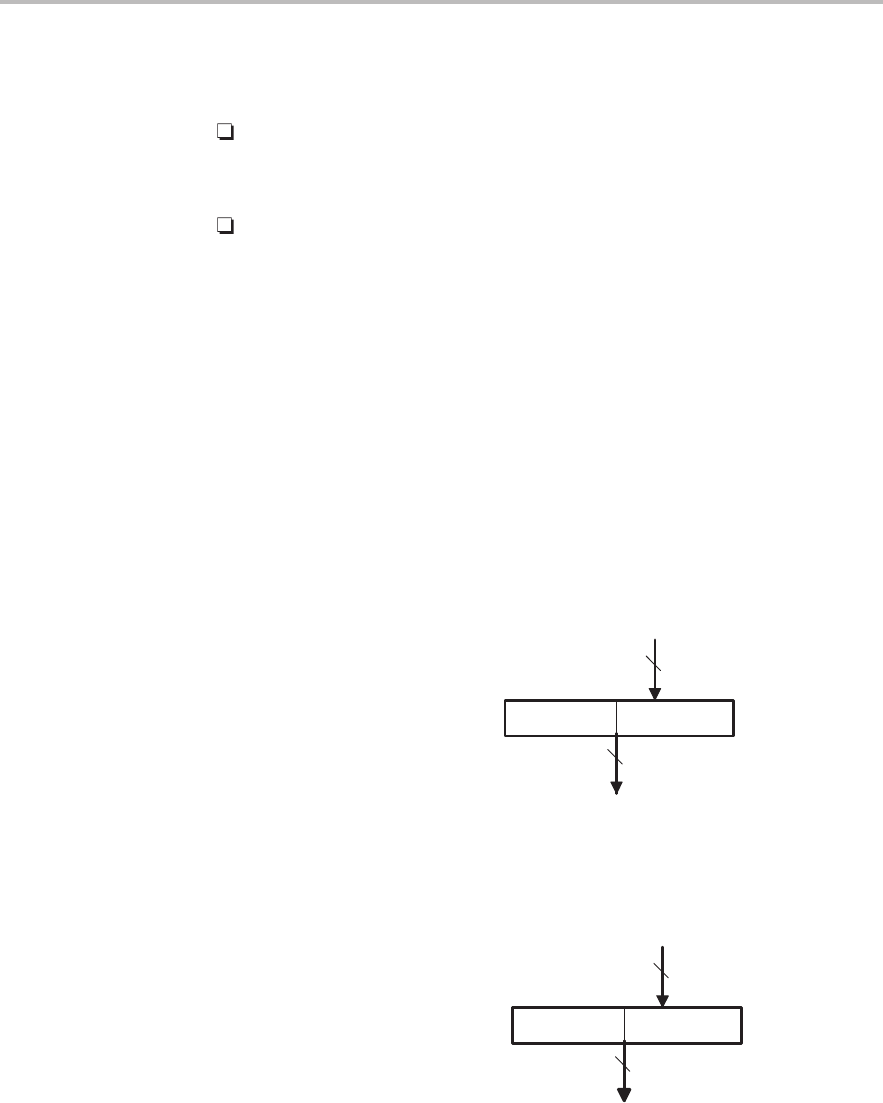
Figure 3–3 shows an example of an input value shifted left by 8 bits for
SXM = 0. The MSBs of the value passed to the CALU are zero filled.
Figure 3–4 shows the same shift but with SXM = 1. The value is sign extended
during the shift.
Figure 3–3. Operation of the Input Shifter for SXM = 0
Output value
after left shift of 8
(SXM = 0)
X X X X A F 1 1
16
Input shifter
accepting the
value
32
0 0 A F 1 1 0 0
A F 1 1
Figure 3–4. Operation of the Input Shifter for SXM = 1
Output value
after left shift of 8
(SXM = 1)
X X X X A F 1 1
16
Input shifter
accepting the
value
32
F F A F 1 1 0 0
A F 1 1