
Calculator User Manual
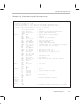
Table Of Contents
- Read This First
- Contents
- Figures
- Tables
- Examples
- Cautions
- Introduction
- Architectural Overview
- Central Processing Unit
- Memory and I/O Spaces
- Program Control
- Addressing Modes
- Assembly Language Instructions
- Instruction Set Summary
- How To Use the Instruction Descriptions
- Instruction Descriptions
- ABS
- ABS
- ADD
- ADD
- ADD
- ADD
- ADDC
- ADDC
- ADDS
- ADDS
- ADDT
- ADDT
- ADRK
- AND
- AND
- AND
- APAC
- APAC
- B
- BACC
- BANZ
- BANZ
- BCND
- BCND
- BIT
- BIT
- BITT
- BITT
- BLDD
- BLDD
- BLDD
- BLDD
- BLDD
- BLPD
- BLPD
- BLPD
- BLPD
- CALA
- CALL
- CC
- CC
- CLRC
- CLRC
- CMPL
- CMPR
- DMOV
- DMOV
- IDLE
- IN
- IN
- INTR
- LACC
- LACC
- LACC
- LACL
- LACL
- LACL
- LACT
- LACT
- LAR
- LAR
- LAR
- LDP
- LDP
- LPH
- LPH
- LST
- LST
- LST
- LST
- LT
- LT
- LTA
- LTA
- LTD
- LTD
- LTD
- LTP
- LTP
- LTS
- LTS
- MAC
- MAC
- MAC
- MAC
- MACD
- MACD
- MACD
- MACD
- MACD
- MAR
- MAR
- MPY
- MPY
- MPY
- MPYA
- MPYA
- MPYS
- MPYS
- MPYU
- MPYU
- NEG
- NEG
- NMI
- NOP
- NORM
- NORM
- NORM
- OR
- OR
- OR
- OUT
- OUT
- PAC
- POP
- POP
- POPD
- POPD
- PSHD
- PSHD
- PUSH
- RET
- RETC
- ROL
- ROR
- RPT
- RPT
- SACH
- SACH
- SACL
- SACL
- SAR
- SAR
- SBRK
- SETC
- SETC
- SFL
- SFR
- SFR
- SPAC
- SPH
- SPH
- SPL
- SPL
- SPLK
- SPLK
- SPM
- SQRA
- SQRA
- SQRS
- SQRS
- SST
- SST
- SUB
- SUB
- SUB
- SUB
- SUBB
- SUBB
- SUBC
- SUBC
- SUBS
- SUBS
- SUBT
- SUBT
- TBLR
- TBLR
- TBLR
- TBLW
- TBLW
- TBLW
- TRAP
- XOR
- XOR
- XOR
- ZALR
- ZALR
- On-Chip Peripherals
- Synchronous Serial Port
- Asynchronous Serial Port
- TMS320C209
- Register Summary
- TMS320C1x/C2x/C2xx/C5x Instruction Set Comparison
- Program Examples
- Submitting ROM Codes to TI
- Design Considerations for Using XDS510 Emulator
- E.1 Designing Your Target System’s Emulator Connector (14-Pin Header)
- E.2 Bus Protocol
- E.3 Emulator Cable Pod
- E.4 Emulator Cable Pod Signal Timing
- E.5 Emulation Timing Calculations
- E.6 Connections Between the Emulator and the Target System
- E.7 Physical Dimensions for the 14-Pin Emulator Connector
- E.8 Emulation Design Considerations
- Glossary
- Index

Task-Specific Program Code
C-11
Program Examples
Example C–7. Implementing a HOLD Operation (hold.asm)
* File: hold.asm *
* Function: HOLD test code *
* Check for HOLDA toggle for HOLD requests in MODE 0 *
* Check for XF toggle on HOLD/INT1 requests in MODE 1 *
.title ” HOLD Test ” ; Title
.mmregs
icr .set 0FFECh ; Interrupt control register in I/O space
icrshdw .set 060h ; scratch pad location
* Interrupt vectors
.text
reset B main ; 0–reset , Branch to main program on reset
int1h B int1_hold ; 1–external interrupt 1 or HOLD
.space 40*16
*********Interrupt service routine ISR for HOLD logic*************************
main: splk #0001h,imr
clrc intm
wait: b wait
int1_hold:
; Perform any desired context save
ldp #0
in icrshdw, icr ; save the contents of ICR register
lacl #010h ; load ACC with mask for MODE bit
and icrshdw ; Filter out all bits except MODE bit
bcnd int1,neq ; Branch if MODE bit is 1, else in HOLD mode
lacc imr, 0 ; load ACC with interrupt mask register
splk #1, imr ; mask all interrupts except interrupt1/HOLD
idle ; enter HOLD mode, issues HOLDA
; and the busses will be in tristate
splk #1, ifr ; Clear HOLD/INT1 flag to prevent
; re–entering HOLD mode
sacl imr ; restore interrupt mask register
; Perform necessary context restore
clrc intm ; enable all interrupts
ret ; return from HOLD interrupt
int1: nop ; Replace this with desired INT1 interrupt
nop ; service routine
setc xf ; Dummy toggle to check the loop entry
clrc xf ; in MODE 1
splk #0001,ifr
clrc intm ; enable all interrupts
ret ; return from interrupts