
Memory Controller User's Guide

www.ti.com
2.13.1 Initializing Configuration Registers
Peripheral Architecture
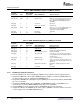
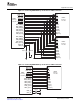
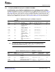
Table 14. DDR2 SDRAM Configuration by MRS Command
DDR2 Memory
Controller DDR2 SDRAM
Address Bus Value Register Bit DDR2 SDRAM Field Function Selection
DDR_A[12] 0 12 Power Down Exit Fast exit
DDR_A[11:9] t_WR 11:9 Write Recovery Write recovery from autoprecharge. Value of 2,
3, 4, 5, or 6 is programmed based on value of
the T_WR bit in the SDRAM timing register
(SDTIMR).
DDR_A[8] 0 8 DLL Reset Out of reset
DDR_A[7] 0 7 Mode: Test or Normal Normal mode
DDR_A[6:4] CL bit 6:4 CAS Latency Value of 2, 3, 4, or 5 is programmed based on
value of the CL bit in the SDRAM bank
configuration register (SDBCR).
DDR_A[3] 0 3 Burst Type Sequential
DDR_A[2:0] 3h 2:0 Burst Length 8
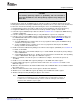
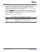
Table 15. DDR2 SDRAM Configuration by EMRS(1) Command
DDR2 Memory
Controller DDR2 SDRAM
Address Bus Value Register Bit DDR2 SDRAM Field Function Selection
DDR_A[12] 0 12 Output Buffer Enable Output buffer enable
DDR_A[11] 0 11 RDQS Enable RDQS disable
DDR_A[10] 1 10 DQS enable Disables differential DQS signaling.
DDR_A[9:7] 0 9:7 OCD Calibration Program Exit OCD calibration
DDR_A[6] 0 6 ODT Value (Rtt) Cleared to 0 to select 75 ohms. This feature is
not supported because the DDR_ODT signal is
not pinned out.
DDR_A[5:3] 0 5:3 Additive Latency 0 cycles of additive latency
DDR_A[2] 1 2 ODT Value (Rtt) Set to 1 to select 75 ohms. This feature is not
supported because the DDR_ODT signal is not
pinned out.
DDR_A[1] 1 1 Output Driver Impedance DDR2 drive strength programmed to weak
(60%).
DDR_A[0] 0 0 DLL enable DLL enable
Perform the following steps when configuring the DDR2 memory controller memory-mapped registers:
1. Program the DDR PHY control register (DDRPHYCR) by setting the read latency (READLAT) bits to
the desired value as well as clearing the DLLPWRDN bit to 0.
2. Program the SDRAM bank configuration register (SDBCR) to the desired value with the TIMUNLOCK
bit set to 1 (unlocked).
3. Program the SDRAM timing register (SDTIMR) and SDRAM timing register 2 (SDTIMR2) to the
desired values to meet the DDR2 SDRAM memory data sheet specification.
4. Program SDBCR to the desired value with the TIMUNLOCK bit cleared to 0 (locked).
5. Program the RR bit in the SDRAM refresh control register (SDRCR) to the desired value to meet the
refresh requirements of the DDR2 SDRAM memory.
DDR2 Memory Controller32 SPRUEM4A – November 2007
Submit Documentation Feedback