
DDR2 Memory Controller User's Guide

www.ti.com
3.2.4 Configuring the DDR2 Memory Controller Control Register (DMCCTL)
Using the DDR2 Memory Controller
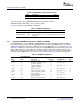
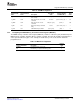
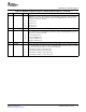
Table 15. SDTIM2 Configuration
DDR2 SDRAM Data
Register Field Sheet Parameter Data Sheet Formula (Register Field
Name Name Description Value Field Must Be ≥ ) Value
T_ODT t
AOND
t
AOND
specifies the ODT 2 (t
CK
cycles) CAS latency - t
AOND
- 1 1
turn-on delay
T_SXNR t
SXNR
Exit self refresh to a non-read 137.5 nS (t
SXNR
× f
DDR2_CLK
) - 1 36
command
T_SXRD t
SXRD
Exit self refresh to a read 200 (t
CK
cycles) (t
SXRD
) - 1 199
command
T_RTP t
RTP
Read to precharge command 7.5 nS (t
RTP
× f
DDR2_CLK
) - 1 1
delay
T_CKE t
CKE
CKE minimum pulse width 3 (t
CK
cycles) (t
CKE
) - 1 2
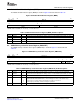
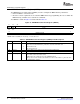
The DDR2 memory controller control register (DMCCTL) contains a read latency (RL) field that helps the
DDR2 memory controller determine when to sample read data. The RL field should be programmed to a
value equal to CAS latency plus 1. For example, if a CAS latency of 4 is used, then RL should be
programmed to 5.
Table 16. DMCCTL Configuration
Register
Register Field Name Description Value
IFRESET Programmed to be out of reset. 0
RL Read latency is equal to CAS latency plus 1. 5
SPRUF85 – October 2007 DSP DDR2 Memory Controller 35
Submit Documentation Feedback