
Digital Signal Processor Product Preview

www.ti.com
PRODUCT PREVIEW
7.9.2 DDR2 Memory Controller Peripheral Register Description(s)
7.9.3 DDR2 Memory Controller Electrical Data/Timing
TMS320C6454
Fixed-Point Digital Signal Processor
SPRS311A – APRIL 2006 – REVISED DECEMBER 2006
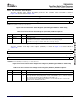
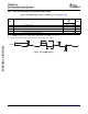
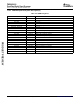
Table 7-40. DDR2 Memory Controller Registers
HEX ADDRESS RANGE ACRONYM REGISTER NAME
7800 0000 MIDR DDR2 Memory Controller Module and Revision Register
7800 0004 DMCSTAT DDR2 Memory Controller Status Register
7800 0008 SDCFG DDR2 Memory Controller SDRAM Configuration Register
7800 000C SDRFC DDR2 Memory Controller SDRAM Refresh Control Register
7800 0010 SDTIM1 DDR2 Memory Controller SDRAM Timing 1 Register
7800 0014 SDTIM2 DDR2 Memory Controller SDRAM Timing 2 Register
7800 0018 - Reserved
7800 0020 BPRIO DDR2 Memory Controller Burst Priority Register
7800 0024 - 7800 004C - Reserved
7800 0050 - 7800 0078 - Reserved
7800 007C - 7800 00BC - Reserved
7800 00C0 - 7800 00E0 - Reserved
7800 00E4 DMCCTL DDR2 Memory Controller Control Register
7800 00E8 - 7800 00FC - Reserved
7800 0100 - 7FFF FFFF - Reserved
The Implementing DDR2 PCB Layout on the TMS320C6454 application report (literature number
SPRAAA7 ) specifies a complete DDR2 interface solution for the C6454 as well as a list of compatible
DDR2 devices. TI has performed the simulation and system characterization to ensure all DDR2 interface
timings in this solution are met; therefore, no electrical data/timing information is supplied here for this
interface.
TI only supports designs that follow the board design guidelines outlined in the SPRAAA7
application report.
148 C64x+ Peripheral Information and Electrical Specifications Submit Documentation Feedback