
Digital Signal Processor Product Preview

www.ti.com
PRODUCT PREVIEW
7.10 External Memory Interface A (EMIFA)
7.10.1 EMIFA Device-Specific Information
TMS320C6454
Fixed-Point Digital Signal Processor
SPRS311A – APRIL 2006 – REVISED DECEMBER 2006
The EMIFA can interface to a variety of external devices or ASICs, including:
• Pipelined and flow-through Synchronous-Burst SRAM (SBSRAM)
• ZBT (Zero Bus Turnaround) SRAM and Late Write SRAM
• Synchronous FIFOs
• Asynchronous memory, including SRAM, ROM, and Flash
Timing analysis must be done to verify all AC timings are met. TI recommends utilizing I/O buffer
information specification (IBIS) to analyze all AC timings.
To properly use IBIS models to attain accurate timing analysis for a given system, see the Using IBIS
Models for Timing Analysis application report (literature number SPRA839 ).
To maintain signal integrity, serial termination resistors should be inserted into all EMIF output signal lines
(for the EMIF output signals, see Table 2-3 , Terminal Functions).
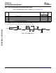
A race condition may exist when certain masters write data to the EMIFA. For example, if master A
passes a software message via a buffer in external memory and does not wait for indication that the write
completes, when master B attempts to read the software message, then the master B read may bypass
the master A write and, thus, master B may read stale data and, therefore, receive an incorrect message.
Some master peripherals (e.g., EDMA3 transfer controllers) will always wait for the write to complete
before signaling an interrupt to the system, thus avoiding this race condition. For masters that do not have
hardware guarantee of write-read ordering, it may be necessary to guarantee data ordering via software.
If master A does not wait for indication that a write is complete, it must perform the following workaround:
1. Perform the required write.
2. Perform a dummy write to the EMIFA module ID and revision register.
3. Perform a dummy read to the EMIFA module ID and revision register.
4. Indicate to master B that the data is ready to be read after completion of the read in step 3. The
completion of the read in step 3 ensures that the previous write was done.
Submit Documentation Feedback C64x+ Peripheral Information and Electrical Specifications 149