
Digital Signal Processor Product Preview

www.ti.com
PRODUCT PREVIEW
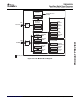
7.11.3 I2C Electrical Data/Timing
TMS320C6454
Fixed-Point Digital Signal Processor
SPRS311A – APRIL 2006 – REVISED DECEMBER 2006
7.11.3.1 Inter-Integrated Circuits (I2C) Timing
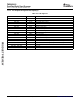
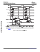
Table 7-52. Timing Requirements for I2C Timings
(1)
(see Figure 7-42 )
-720
-850
-1000
NO. UNIT
STANDARD MODE FAST MODE
MIN MAX MIN MAX
1 t
c(SCL)
Cycle time, SCL 10 2.5 µ s
Setup time, SCL high before SDA low (for a
2 t
su(SCLH-SDAL)
4.7 0.6 µ s
repeated START condition)
Hold time, SCL low after SDA low (for a
3 t
h(SCLL-SDAL)
4 0.6 µ s
START and a repeated START condition)
4 t
w(SCLL)
Pulse duration, SCL low 4.7 1.3 µ s
5 t
w(SCLH)
Pulse duration, SCL high 4 0.6 µ s
6 t
su(SDAV-SDLH)
Setup time, SDA valid before SCL high 250 100
(2)
ns
Hold time, SDA valid after SCL low (For I
2
C
7 t
h(SDA-SDLL)
0
(3)
0
(3)
0.9
(4)
µ s
bus™ devices)
Pulse duration, SDA high between STOP and
8 t
w(SDAH)
START 4.7 1.3 µ s
conditions
9 t
r(SDA)
Rise time, SDA 1000 20 + 0.1C
b
(5)
300 ns
10 t
r(SCL)
Rise time, SCL 1000 20 + 0.1C
b
(5)
300 ns
11 t
f(SDA)
Fall time, SDA 300 20 + 0.1C
b
(5)
300 ns
12 t
f(SCL)
Fall time, SCL 300 20 + 0.1C
b
(5)
300 ns
Setup time, SCL high before SDA high (for
13 t
su(SCLH-SDAH)
4 0.6 µ s
STOP condition)
14 t
w(SP)
Pulse duration, spike (must be suppressed) 0 50 ns
15 C
b
(5)
Capacitive load for each bus line 400 400 pF
(1) The I2C pins SDA and SCL do not feature fail-safe I/O buffers. These pins could potentially draw current when the device is powered
down.
(2) A Fast-mode I
2
C-bus™ device can be used in a Standard-mode I
2
C-bus™ system, but the requirement t
su(SDA-SCLH)
≥ 250 ns must then
be met. This will automatically be the case if the device does not stretch the LOW period of the SCL signal. If such a device does stretch
the LOW period of the SCL signal, it must output the next data bit to the SDA line t
r
max + t
su(SDA-SCLH)
= 1000 + 250 = 1250 ns
(according to the Standard-mode I
2
C-Bus Specification) before the SCL line is released.
(3) A device must internally provide a hold time of at least 300 ns for the SDA signal (referred to the V
IHmin
of the SCL signal) to bridge the
undefined region of the falling edge of SCL.
(4) The maximum t
h(SDA-SCLL)
has only to be met if the device does not stretch the low period [t
w(SCLL)
] of the SCL signal.
(5) C
b
= total capacitance of one bus line in pF. If mixed with HS-mode devices, faster fall-times are allowed.
Submit Documentation Feedback C64x+ Peripheral Information and Electrical Specifications 163