
Digital Signal Processor Product Preview

www.ti.com
PRODUCT PREVIEW
TMS320C6454
Fixed-Point Digital Signal Processor
SPRS311A – APRIL 2006 – REVISED DECEMBER 2006
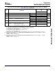
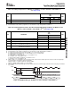
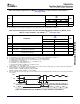
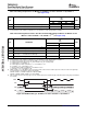
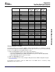
Table 7-60. Switching Characteristics Over Recommended Operating Conditions for McBSP
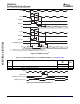
(see Figure 7-52 ) (continued)
-720
-850
NO. PARAMETER UNIT
-1000
MIN MAX
3 t
w(CKRX)
Pulse duration, CLKR/X high or CLKR/X low CLKR/X int C – 1
(7)
C + 1
(7)
ns
4 t
d(CKRH-FRV)
Delay time, CLKR high to internal FSR valid CLKR int –2.1 3.3 ns
CLKX int –1.7 3
9 t
d(CKXH-FXV)
Delay time, CLKX high to internal FSX valid ns
CLKX ext 1.7 9
CLKX int –3.9 4
Disable time, DX high impedance following
12 t
dis(CKXH-DXHZ)
ns
last data bit from CLKX high
CLKX ext 2.1 9
CLKX int –3.9 + D1
(8)
4 + D2
(8)
13 t
d(CKXH-DXV)
Delay time, CLKX high to DX valid ns
CLKX ext 2.1 + D1
(8)
9 + D2
(8)
Delay time, FSX high to DX valid FSX int –2.3 + D1
(9)
5.6 + D2
(9)
14 t
d(FXH-DXV)
ns
ONLY applies when in data
FSX ext 1.9 + D1
(9)
9 + D2
(9)
delay 0 (XDATDLY = 00b) mode
(7) C = H or L
S = sample rate generator input clock = 6P if CLKSM = 1 (P = 1/CPU clock frequency)
S = sample rate generator input clock = P_clks if CLKSM = 0 (P_clks = CLKS period)
H = CLKX high pulse width = (CLKGDV/2 + 1) * S if CLKGDV is even
H = (CLKGDV + 1)/2 * S if CLKGDV is odd
L = CLKX low pulse width = (CLKGDV/2) * S if CLKGDV is even
L = (CLKGDV + 1)/2 * S if CLKGDV is odd
CLKGDV should be set appropriately to ensure the McBSP bit rate does not exceed the maximum limit (see (4) above).
(8) Extra delay from CLKX high to DX valid applies only to the first data bit of a device, if and only if DXENA = 1 in SPCR.
if DXENA = 0, then D1 = D2 = 0
if DXENA = 1, then D1 = 6P, D2 = 12P
(9) Extra delay from FSX high to DX valid applies only to the first data bit of a device, if and only if DXENA = 1 in SPCR.
if DXENA = 0, then D1 = D2 = 0
if DXENA = 1, then D1 = 6P, D2 = 12P
Submit Documentation Feedback C64x+ Peripheral Information and Electrical Specifications 181