
Digital Signal Processor Product Preview

www.ti.com
PRODUCT PREVIEW
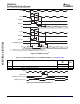
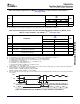
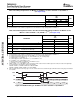
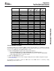
Bit 0 Bit(n-1) (n-2) (n-3) (n-4)
Bit 0 Bit(n-1) (n-2) (n-3) (n-4)
4
376
21
CLKX
FSX
DX
DR
5
TMS320C6454
Fixed-Point Digital Signal Processor
SPRS311A – APRIL 2006 – REVISED DECEMBER 2006
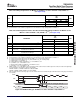
Table 7-64. Timing Requirements for McBSP as SPI Master or Slave: CLKSTP = 11b, CLKXP = 0
(1) (2)
(see Figure 7-55 )
-720
-850
-1000
NO. UNIT
MASTER SLAVE
MIN MAX MIN MAX
4 t
su(DRV-CKXH)
Setup time, DR valid before CLKX high 12 2 – 18P ns
5 t
h(CKXH-DRV)
Hold time, DR valid after CLKX high 4 5 + 36P ns
(1) P = 1/CPU clock frequency in ns. For example, when running parts at 1000 MHz, use P = 1 ns.
(2) For all SPI Slave modes, CLKG is programmed as 1/6 of the CPU clock by setting CLKSM = CLKGDV = 1.
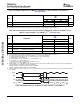
Table 7-65. Switching Characteristics Over Recommended Operating Conditions for McBSP as SPI
Master or Slave: CLKSTP = 11b, CLKXP = 0
(1) (2)
(see Figure 7-55 )
-720
-850
-1000
NO. PARAMETER UNIT
MASTER
(3)
SLAVE
MIN MAX MIN MAX
1 t
h(CKXL-FXL)
Hold time, FSX low after CLKX low
(4)
L – 2 L + 3 ns
2 t
d(FXL-CKXH)
Delay time, FSX low to CLKX high
(5)
T – 2 T + 3 ns
3 t
d(CKXL-DXV)
Delay time, CLKX low to DX valid –2 4 18P + 2.8 30P + 17 ns
Disable time, DX high impedance following
6 t
dis(CKXL-DXHZ)
–2 4 18P + 3 30P + 17 ns
last data bit from CLKX low
7 t
d(FXL-DXV)
Delay time, FSX low to DX valid H – 2 H + 4 12P + 2 24P + 17 ns
(1) P = 1/CPU clock frequency in ns. For example, when running parts at 1000 MHz, use P = 1 ns.
(2) For all SPI Slave modes, CLKG is programmed as 1/6 of the CPU clock by setting CLKSM = CLKGDV = 1.
(3) S = Sample rate generator input clock = 6P if CLKSM = 1 (P = 1/CPU clock frequency)
S = Sample rate generator input clock = P_clks if CLKSM = 0 (P_clks = CLKS period)
T = CLKX period = (1 + CLKGDV) * S
H = CLKX high pulse width = (CLKGDV/2 + 1) * S if CLKGDV is even
H = (CLKGDV + 1)/2 * S if CLKGDV is odd
L = CLKX low pulse width = (CLKGDV/2) * S if CLKGDV is even
L = (CLKGDV + 1)/2 * S if CLKGDV is odd
(4) FSRP = FSXP = 1. As a SPI Master, FSX is inverted to provide active-low slave-enable output. As a Slave, the active-low signal input
on FSX and FSR is inverted before being used internally.
CLKXM = FSXM = 1, CLKRM = FSRM = 0 for Master McBSP
CLKXM = CLKRM = FSXM = FSRM = 0 for Slave McBSP
(5) FSX should be low before the rising edge of clock to enable Slave devices and then begin a SPI transfer at the rising edge of the Master
clock (CLKX).
Figure 7-55. McBSP Timing as SPI Master or Slave: CLKSTP = 11b, CLKXP = 0
184 C64x+ Peripheral Information and Electrical Specifications Submit Documentation Feedback