
Digital Signal Processor Product Preview

www.ti.com
PRODUCT PREVIEW
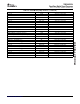
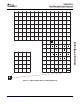
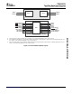
A. This pin functions as GP[1] by default. For more details, see the Device Configuration section of this document.
B. These McBSP1 peripheral pins are muxed with the GPIO peripheral pins and by default these signals function as GPIO peripheral pins. For
more details, see the Device Configuration section of this document.
C. These PCI peripheral pins are muxed with the GPIO peripheral pins and by default these signals function as GPIO peripheral pins. For more
details, see the Device Configuration section of this document.
GPIO
General-Purpose Input/Output 0 (GPIO) Port
CLKX1/GP[3]
(B)
PCBE0/GP[2]
(C)
SYSCLK4/GP[1]
(A)
PREQ/GP[15]
(C)
PINTA/GP[14]
(C)
PRST/GP[13]
(C)
PGNT/GP[12]
(C)
FSX1/GP[11]
(B)
FSR1/GP[10]
(B)
DX1/GP[9]
(B)
DR1/GP[8]
(B)
GP[7]
GP[6]
GP[5]
GP[4]
CLKR1/GP[0]
(B)
Timers (64-Bit)
TINPL1
Timer 1
Timer 0
TOUTL1
TINPL0
TOUTL0
TMS320C6454
Fixed-Point Digital Signal Processor
SPRS311A – APRIL 2006 – REVISED DECEMBER 2006
Figure 2-7. Timers/GPIO Peripheral Signals
Submit Documentation Feedback Device Overview 19