
Digital Signal Processor Product Preview

www.ti.com
PRODUCT PREVIEW
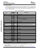
2.7 Terminal Functions
TMS320C6454
Fixed-Point Digital Signal Processor
SPRS311A – APRIL 2006 – REVISED DECEMBER 2006
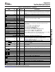
The terminal functions table (Table 2-3 ) identifies the external signal names, the associated pin (ball)
numbers along with the mechanical package designator, the pin type (I, O/Z, or I/O/Z), whether the pin
has any internal pullup/pulldown resistors, and a functional pin description. For more detailed information
on device configuration, peripheral selection, multiplexed/shared pins, and pullup/pulldown resistors, see
Section 3 , Device Configuration.
Table 2-3. Terminal Functions
SIGNAL
TYPE
(1)
IPD/IPU
(2)
DESCRIPTION
NAME NO.
CLOCK/PLL CONFIGURATIONS
CLKIN1 N28 I IPD Clock Input for PLL1.
CLKIN2 G3 I IPD Clock Input for PLL2.
PLLV1 T29 A 1.8-V I/O supply voltage for PLL1
PLLV2 A5 A 1.8-V I/O supply voltage for PLL2
SYSCLK4 is the clock output at 1/8 of the device speed ( O/Z) or this pin can be
SYSCLK4/GP[1]
(3)
AJ13 I/O/Z IPD
programmed as the GP1 pin ( I/O/Z) [default].
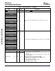
JTAG EMULATION
TMS AJ10 I IPU JTAG test-port mode select
TDO AH8 O/Z IPU JTAG test-port data out
TDI AH9 I IPU JTAG test-port data in
TCK AJ9 I IPU JTAG test-port clock
JTAG test-port reset. For IEEE 1149.1 JTAG compatibility, see the IEEE
TRST AH7 I IPD
1149.1 JTAG compatibility statement portion of this document.
EMU0
(4)
AF7 I/O/Z IPU Emulation pin 0
EMU1
(4)
AE11 I/O/Z IPU Emulation pin 1
EMU2 AG9 I/O/Z IPU Emulation pin 2
EMU3 AF10 I/O/Z IPU Emulation pin 3
EMU4 AF9 I/O/Z IPU Emulation pin 4
EMU5 AE12 I/O/Z IPU Emulation pin 5
EMU6 AG8 I/O/Z IPU Emulation pin 6
EMU7 AF12 I/O/Z IPU Emulation pin 7
EMU8 AF11 I/O/Z IPU Emulation pin 8
EMU9 AH13 I/O/Z IPU Emulation pin 9
EMU10 AD10 I/O/Z IPU Emulation pin 10
EMU11 AD12 I/O/Z IPU Emulation pin 11
EMU12 AE10 I/O/Z IPU Emulation pin 12
EMU13 AD8 I/O/Z IPU Emulation pin 13
EMU14 AF13 I/O/Z IPU Emulation pin 14
EMU15 AE9 I/O/Z IPU Emulation pin 15
EMU16 AH12 I/O/Z IPU Emulation pin 16
EMU17 AH10 I/O/Z IPU Emulation pin 17
EMU18 AE13 I/O/Z IPU Emulation pin 18
RESETS, INTERRUPTS, AND GENERAL-PURPOSE INPUT/OUTPUTS
RESET AG14 I Device reset
(1) I = Input, O = Output, Z = High impedance, S = Supply voltage, GND = Ground, A = Analog signal
(2) IPD = Internal pulldown, IPU = Internal pullup. For most systems, a 1-k Ω resistor can be used to oppose the IPU/IPD. For more detailed
information on pullup/pulldown resistors and situations where external pullup/pulldown resistors are required, see Section 3.7 ,
Pullup/Pulldown Resistors.
(3) These pins are multiplexed pins. For more details, see Section 3 , Device Configuration.
(4) The C6454 DSP does not require external pulldown resistors on the EMU0 and EMU1 pins for normal or boundary-scan operation.
Device Overview24 Submit Documentation Feedback