
Digital Signal Processor Product Preview
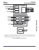
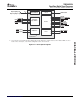

www.ti.com
PRODUCT PREVIEW
TMS320C6454
Fixed-Point Digital Signal Processor
SPRS311A – APRIL 2006 – REVISED DECEMBER 2006
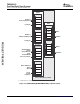
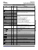
Table 2-3. Terminal Functions (continued)
SIGNAL
TYPE
(1)
IPD/IPU
(2)
DESCRIPTION
NAME NO.
Nonmaskable interrupt, edge-driven (rising edge)
Any noise on the NMI pin may trigger an NMI interrupt; therefore, if the NMI pin
NMI AH4 I IPD
is not used, it is recommended that the NMI pin be grounded versus relying on
the IPD.
RESETSTAT AE14 O Reset Status pin. The RESETSTAT pin indicates when the device is in reset
POR AF14 I Power on reset.
GP[7] AG2 I/O/Z IPD
GP[6] AG3 I/O/Z IPD
General-purpose input/output (GPIO) pins ( I/O/Z).
GP[5] AJ2 I/O/Z IPD
GP[4] AH2 I/O/Z IPD
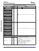
PREQ/GP[15] P2 I/O/Z
PINTA
(5)
/GP[14] P3 I/O/Z
PCI peripheral pins or general-purpose input/output (GPIO) [15:12, 2] pins
PRST/GP[13] R5 I/O/Z
( I/O/Z) [default]
PGNT/GP[12] R4 I/O/Z
PCI bus request ( O/Z) or GP[15] ( I/O/Z) [default]
PCI interrupt A ( O/Z) or GP[14] ( I/O/Z) [default]
FSX1/GP[11] AG4 I/O/Z IPD
PCI reset ( I) or GP[13] ( I/O/Z) [default]
FSR1/GP[10] AE5 I/O/Z IPD
PCI bus grant ( I) or GP[12] ( I/O/Z) [default]
PCI command/byte enable 0 ( I/O/Z) or GP[2] ( I/O/Z) [default]
DX1/GP[9] AG5 I/O/Z IPD
DR1/GP[8] AH5 I/O/Z IPD
McBSP1 transmit clock ( I/O/Z) or GP[3] ( I/O/Z) [default]
McBSP1 receive clock ( I/O/Z) or GP[0] ( I/O/Z) [default]
CLKX1/GP[3] AF5 I/O/Z IPD
GP[1] pin ( I/O/Z). SYSCLK4 is the clock output at 1/8 of the device speed ( O/Z)
PCBE0/GP[2] P1 I/O/Z
or this pin can be programmed as a GP[1] pin ( I/O/Z) [default].
SYSCLK4/GP[1]
(3)
AJ13 O/Z IPD
CLKR1/GP[0] AF4 I/O/Z IPD
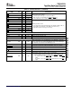
HOST-PORT INTERFACE (HPI) or PERIPHERAL COMPONENT INTERCONNECT (PCI)
PCI enable pin. This pin controls the selection (enable/disable) of the HPI and
GP[15:8], or PCI peripherals. This pin works in conjunction with the
PCI_EN Y29 I IPD
MCBSP 1_EN (AEA5 pin) to enable/disable other peripherals (for more details,
see Section 3 , Device Configuration).
HINT/ PFRAME U3 I/O/Z Host interrupt from DSP to host ( O/Z) or PCI frame ( I/O/Z)
Host control - selects between control, address, or data registers ( I) [default] or
HCNTL1/ PDEVSEL U4 I/O/Z
PCI device select ( I/O/Z)
Host control - selects between control, address, or data registers ( I) [default] or
HCNTL0/ PSTOP U5 I/O/Z
PCI stop ( I/O/Z)
Host half-word select - first or second half-word (not necessarily high or low
HHWIL/PCLK V3 I/O/Z order)
[For HPI16 bus width selection only] ( I) [default] or PCI clock ( I)
HR/ W/ PCBE2 T5 I/O/Z Host read or write select ( I) [default] or PCI command/byte enable 2 ( I/O/Z)
HAS/PPAR T3 I/O/Z Host address strobe ( I) [default] or PCI parity ( I/O/Z)
HCS/ PPERR U6 I/O/Z Host chip select ( I) [default] or PCI parity error ( I/O/Z)
HDS1/ PSERR
(5)
U2 I/O/Z Host data strobe 1 ( I) [default] or PCI system error ( I/O/Z)
HDS2/ PCBE1 U1 I/O/Z Host data strobe 2 ( I) [default] or PCI command/byte enable 1 ( I/O/Z)
HRDY/ PIRDY T4 I/O/Z Host ready from DSP to host ( O/Z) [default] or PCI initiator ready ( I/O/Z)
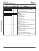
PREQ/GP[15] P2 I/O/Z PCI bus request ( O/Z) or GP[15] ( I/O/Z) [default]
PINTA
(5)
/GP[14] P3 I/O/Z PCI interrupt A ( O/Z) or GP[14] ( I/O/Z) default]
PRST/GP[13] R5 I/O/Z PCI reset ( I) or GP[13] ( I/O/Z) [default]
PGNT/GP[12] R4 I/O/Z PCI bus grant ( I) or GP[12] ( I/O/Z)[default]
PCBE0/GP[2] P1 I/O/Z PCI command/byte enable 0 ( I/O/Z) or GP[2] ( I/O/Z)[default]
PCBE3 P5 I/O/Z PCI command/byte enable 3 ( I/O/Z). By default, this pin has no function.
PIDSEL R3 I PCI initialization device select ( I). By default, this pin has no function.
(5) These pins function as open-drain outputs when configured as PCI pins.
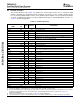
Submit Documentation Feedback Device Overview 25