
Digital Signal Processor Product Preview

www.ti.com
PRODUCT PREVIEW
TMS320C6454
Fixed-Point Digital Signal Processor
SPRS311A – APRIL 2006 – REVISED DECEMBER 2006
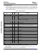
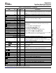
Table 2-3. Terminal Functions (continued)
SIGNAL
TYPE
(1)
IPD/IPU
(2)
DESCRIPTION
NAME NO.
ACE5 V27 O/Z IPU
EMIFA memory space enables
ACE4 V28 O/Z IPU
• Enabled by bits 28 through 31 of the word address
ACE3 W26 O/Z IPU
• Only one pin is asserted during any external data access
Note: The C6454 device does not have ACE0 and ACE1 pins
ACE2 W27 O/Z IPU
ABE7 W29 O/Z IPU
ABE6 K26 O/Z IPU
ABE5 L29 O/Z IPU
EMIFA byte-enable control
ABE4 L28 O/Z IPU
• Decoded from the low-order address bits. The number of address bits or
byte enables used depends on the width of external memory.
ABE3 AA29 O/Z IPU
• Byte-write enables for most types of memory.
ABE2 AA28 O/Z IPU
ABE1 AA25 O/Z IPU
ABE0 AA26 O/Z IPU
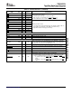
EMIFA (64-BIT) - BUS ARBITRATION
AHOLDA N26 O IPU EMIFA hold-request-acknowledge to the host
AHOLD R29 I IPU EMIFA hold request from the host
ABUSREQ L27 O IPU EMIFA bus request output
EMIFA (64-BIT) - ASYNCHRONOUS/SYNCHRONOUS MEMORY CONTROL
EMIFA external input clock. The EMIFA input clock (AECLKIN or SYSCLK4
AECLKIN N29 I IPD clock) is selected at reset via the pullup/pulldown resistor on the AEA[15] pin.
Note: AECLKIN is the default for the EMIFA input clock.
AECLKOUT V29 O/Z IPD EMIFA output clock [at EMIFA input clock (AECLKIN or SYSCLK4) frequency]
Asynchronous memory write-enable/Programmable synchronous interface
AAWE/ ASWE AB25 O/Z IPU
write-enable
AARDY K29 I IPU Asynchronous memory ready input
AR/ W W25 O/Z IPU Asynchronous memory read/write
AAOE/ ASOE Y28 O/Z IPU Asynchronous/Programmable synchronous memory output-enable
Programmable synchronous address strobe or read-enable
• For programmable synchronous interface, the r_enable field in the Chip
Select x Configuration Register selects between ASADS and ASRE:
ASADS/ ASRE R26 O/Z IPU
– If r_enable = 0, then the ASADS/ ASRE signal functions as the ASADS
signal.
– If r_enable = 1, then the ASADS/ ASRE signal functions as the ASRE
signal.
Submit Documentation Feedback Device Overview 27