
Digital Signal Processor Product Preview

www.ti.com
PRODUCT PREVIEW
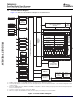
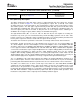
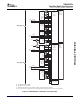
1.3 Functional Block Diagram
L2 Memory Controller
(Memory Protect/
Bandwidth Mgmt)
DDR2
Mem Ctlr
System
(B)
C64x+ DSP Core
Data Path B
B Register File
B31−B16
B15−B0
Instruction Fetch
Data Path A
A Register File
A31−A16
A15−A0
Device
Configuration
Logic
.L1 .S1
.M1
xx
xx
.D1 .D2
.M2
xx
xx
.S2 .L2
64
SBSRAM
SRAM
L1P Cache Direct-Mapped
32K Bytes
L1D Cache
2-Way
Set-Associative
32K Bytes Total
C6454
Primary Switched Central Resource
PLL1 and
PLL1
Controller
EMIFA
ZBT SRAM
HI
Boot Configuration
ROM/FLASH
I/O Devices
I2C
GPIO16
(B)
16
McBSP0
(A)
Internal DMA
(IDMA)
M
e
g
a
m
o
d
u
l
e
L2
Cache
Memory
1048K
Bytes
L1P Memory Controller (Memory Protect/Bandwidth Mgmt)
McBSP1
(A)
HPI (32/16)
(B)
Instruction
Decode
16-/32-bit
Instruction Dispatch
Control Registers
In-Circuit Emulation
DDR2 SDRAM
32
LO
Timer1
(C)
HI
LO
Timer0
(C)
PLL2 and
PLL2
Controller
(D)
EMAC
10/100/1000
SPLOOP Buffer
Power Control
L1D Memory Controller (Memory Protect/Bandwidth Mgmt)
Interrupt and Exception Controller
EDMA 3.0
L2 ROM
32K
Bytes
(E)
Secondary
Switched Central
Resource
A. McBSPs: Framing Chips − H.100, MVIP, SCSA, T1, E1; AC97 Devices; SPI Devices; Codecs
B. The PCI peripheral pins are muxed with some of the HPI peripheral pins. For more detailed information, see the Device Configuration section
of this document.
C. Each of the TIMER peripherals (TIMER1 and TIMER0) is configurable as either two 64-bit general-purpose timers or two 32-bit general-purpose
timers or a watchdog timer.
D. The PLL2 controller also generates clocks for the EMAC.
E. When accessing the internal ROM of the DSP, the CPU frequency must always be less than 750 MHz.
MDIO
RMGII
(D)
GMII
RMII
MII
PCI66
(B)
TMS320C6454
Fixed-Point Digital Signal Processor
SPRS311A – APRIL 2006 – REVISED DECEMBER 2006
Figure 1-2 shows the functional block diagram of the C6454 device.
Figure 1-2. Functional Block Diagram
TMS320C6454 Fixed-Point Digital Signal Processor4 Submit Documentation Feedback