
Computer Hardware User Manual

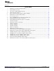


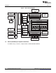

L1 S1 M1 D1
Data path A
Register file A
Register file B
D2
Data path B
S2M2 L2
L1 data memory controller
Cache control
Memory protection
Interrupt
and exception
controller
Power control
Instruction decode
16/32−bit instruction dispatch
Instruction fetch
SPLOOP buffer
C64x+ CPU
IDMA
Bandwidth management
Cache control
L1 program memory controller
Advanced
event
triggering
(AET)
L2 memory
controller
Bandwidth
management
Memory
protection
registers
Configuration
L1P
cache/SRAM
L1D
cache/SRAM
PLL2
DDR2 memory
EMIFA
Other
peripherals
EDMA
Boot
configuration
Switched central resource
PLL2
L2 memory
controller
controller
memory
External
controller
DMA
Master
DMA
Slave
Cache
control
Bandwidth management
Memory protection
Introduction
www.ti.com
Figure 1. Device Block Diagram
1.4 Industry Standard(s) Compliance Statement
The DDR2 memory controller is compliant with the JESD79-2B DDR2 SDRAM.
10
C6455/C6454 DDR2 Memory Controller SPRU970G– December 2005– Revised June 2011
Submit Documentation Feedback
Copyright © 2005–2011, Texas Instruments Incorporated