
Computer Hardware User Manual


Using the DDR2 Memory Controller
www.ti.com
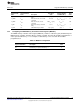
Table 12 displays the DDR2-533 refresh rate specification.
Table 12. DDR2 Memory Refresh Specification
Symbol Description Value
t
REF
Average Periodic Refresh Interval 7.8 μs
Therefore, the value for the REFRESH-RATE can be calculated as follows:
REFRESH_RATE = 250 MHz × 7.8 μs = 1950 = 79Eh
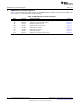
Table 13 shows the resulting SDRFC configuration.
Table 13. SDRFC Configuration
Field Value Function Selection
SR 0 DDR2 memory controller is not in self-refresh mode.
REFRESH_RATE 79Eh Set to 79Eh DDR2 clock cycles to meet the DDR2 memory refresh rate
requirement.
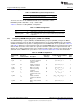
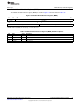
3.2.3 Configuring SDRAM Timing Registers (SDTIM1 and SDTIM2)
The SDRAM timing 1 register (SDTIM1) and SDRAM timing 2 register (SDTIM2) configure the DDR2
memory controller to meet the data sheet timing parameters of the attached DDR2 device. Each field in
SDTIM1 and SDTIM2 corresponds to a timing parameter in the DDR2 data sheet specification. Table 14
and Table 15 display the register field name and corresponding DDR2 data sheet parameter name along
with the data sheet value. These tables also provide a formula to calculate the register field value and
displays the resulting calculation. Each of the equations include a minus 1 because the register fields are
defined in terms of DDR2 clock cycles minus 1. See Section 4.5 and Section 4.6 for more information.
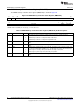
Table 14. SDTIM1 Configuration
DDR2 SDRAM
Register Field Data Sheet Data Sheet Formula (Register Field Must Field
Name Parameter Name Description Value (ns) Be ≥) Value
T_RFC t
RFC
Refresh cycle time 127.5 (t
RFC
× f
DDR2_CLK
) - 1 31
T_RP t
RP
Precharge command to 15 (t
RP
× f
DDR2_CLK
) - 1 3
refresh or activate
command
T_RCD t
RCD
Activate command to 15 (t
RCD
× f
DDR2_CLK
) - 1 3
read/write command
T_WR t
WR
Write recovery time 15 (t
WR
× f
DDR2_CLK
) - 1 3
T_RAS t
RAS
Active to precharge 45 (t
RAC
× f
DDR2_CLK
) - 1 11
command
T_RC t
RC
Activate to Activate 60 (t
RC
× f
DDR2_CLK
) - 1 14
command in the same
bank
T_RRD t
RRD
Activate to Activate 10 ( (4*t
rrd
+ 2*t
ck
) / (4*t
ck
) ) - 1 2
command in a different
bank
T_WTR t
WTR
Write to read command 7.5 (t
WTR
× f
DDR2_CLK
) - 1 1
delay
36
C6455/C6454 DDR2 Memory Controller SPRU970G– December 2005– Revised June 2011
Submit Documentation Feedback
Copyright © 2005–2011, Texas Instruments Incorporated