
Computer Hardware User Manual


www.ti.com
List of Figures
1 Device Block Diagram .................................................................................................... 10
2 DDR2 Memory Controller Signals ....................................................................................... 12
3 DDR2 MRS and EMRS Command...................................................................................... 14
4 Refresh Command ........................................................................................................ 15
5 ACTV Command........................................................................................................... 16
6 DCAB Command .......................................................................................................... 17
7 DEAC Command .......................................................................................................... 18
8 DDR2 READ Command .................................................................................................. 19
9 DDR2 WRT Command ................................................................................................... 20
10 Byte Alignment............................................................................................................. 21
11 Logical Address-to-DDR2 SDRAM Address Map for 32-Bit SDRAM............................................... 22
12 Logical Address-to-DDR2 SDRAM Address Map for 16-bit SDRAM ............................................... 22
13 Logical Address-to-DDR2 SDRAM Address Map ..................................................................... 23
14 DDR2 SDRAM Column, Row, and Bank Access ..................................................................... 24
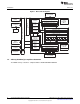
15 DDR2 Memory Controller FIFO Block Diagram ....................................................................... 25
16 Connecting to Two 16-Bit DDR2 SDRAM Devices ................................................................... 32
17 Connecting to a Single 16-Bit DDR2 SDRAM Device ................................................................ 33
18 Connecting to Two 8-Bit DDR2 SDRAM Devices..................................................................... 34
19 Module ID and Revision Register (MIDR).............................................................................. 39
20 DDR2 Memory Controller Status Register (DMCSTAT).............................................................. 40
21 SDRAM Configuration Register (SDCFG) ............................................................................. 41
22 SDRAM Refresh Control Register (SDRFC)........................................................................... 43
23 SDRAM Timing 1 Register (SDTIM1)................................................................................... 44
24 SDRAM Timing 2 Register (SDTIM2)................................................................................... 46
25 Burst Priority Register (BPRIO).......................................................................................... 47
26 DDR2 Memory Controller Control Register (DMCCTL) .............................................................. 48
4
List of Figures SPRU970G– December 2005– Revised June 2011
Submit Documentation Feedback
Copyright © 2005–2011, Texas Instruments Incorporated