
Floating Point Digital Signal Processor Specification Sheet

SPRS293A − OCTOBER 2005 − REVISED NOVEMBER 2005
21
POST OFFICE BOX 1443 • HOUSTON, TEXAS 77251−1443
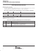
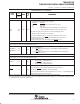
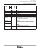
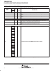
Table 14. Device Configurations Pins at Device Reset
(LENDIAN, EMIFBE, BOOTMODE[1:0], and CLKMODE0)
CONFIGURATION
PIN
GDP/ZDP FUNCTIONAL DESCRIPTION
EMIFBE C15
EMIF Big Endian mode correctness (EMIFBE)
When Big Endian mode is selected (LENDIAN = 0), for proper device operation the
EMIFBE
pin must be externally pulled low.
This new functionality does not affect systems using the current default value of C15 pin=1. For
more detailed information on the Big Endian mode correctness, see the EMIF Big Endian Mode
Correctness portion of this data sheet.
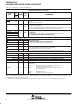
LENDIAN B17
Device Endian mode (LEND)
0 – System operates in Big Endian mode.
The EMIFBE
pin must be pulled low.
1 − System operates in Little Endian mode (default)
BOOTMODE[1:0] C19, C20
Bootmode Configuration Pins (BOOTMODE)
00 – Emulation boot
01 – CE1 width 8-bit, Asynchronous external ROM boot with default
timings (default mode)
10 − CE1
width 16-bit, Asynchronous external ROM boot with default
timings
11 − Reserved, do not use
For more detailed information on these bootmode configurations, see the bootmode section of
this data sheet.
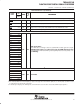
CLKMODE0 C4
Clock generator input clock source select
0 – Reserved. Do not use.
1 − CLKIN square wave [default]
For proper device operation, this pin must be either left unconnected or externally pulled up
with a 1-kΩ resistor.