
Floating Point Digital Signal Processor Specification Sheet

SPRS293A − OCTOBER 2005 − REVISED NOVEMBER 2005
22
POST OFFICE BOX 1443 • HOUSTON, TEXAS 77251−1443
DEVICE CONFIGURATIONS (CONTINUED)
DEVCFG register description
The device configuration register (DEVCFG) allows the user control of the EMIF input clock source. For more
detailed information on the DEVCFG register control bits, see Table 15 and Table 16.
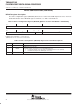
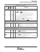
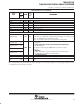
Table 15. Device Configuration Register (DEVCFG) [Address location: 0x019C0200 − 0x019C02FF]
31 16
Reserved
†
RW-0
15
543 0
Reserved
†
EKSRC Reserved
†
RW-0 R/W-0 R/W-0
Legend: R/W = Read/Write; -n = value after reset
†
Do not write non-zero values to these bit locations.
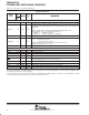
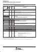
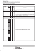
Table 16. Device Configuration (DEVCFG) Register Selection Bit Descriptions
BIT # NAME DESCRIPTION
31:5 Reserved Reserved. Do not write non-zero values to these bit locations.
4 EKSRC
EMIF input clock source bit.
Determines which clock signal is used as the EMIF input clock.
0 = SYSCLK3 (from the clock generator) is the EMIF input clock source (default)
1 = ECLKIN external pin is the EMIF input clock source
3:0 Reserved Reserved. Do not write non-zero values to these bit locations.