
Floating Point Digital Signal Processor Specification Sheet

SPRS293A − OCTOBER 2005 − REVISED NOVEMBER 2005
26
POST OFFICE BOX 1443 • HOUSTON, TEXAS 77251−1443
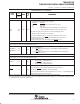
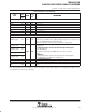
Terminal Functions (Continued)
SIGNAL
PIN
NO.
TYPE
†
IPD/
‡
DESCRIPTION
SIGNAL
NAME
GDP/
ZDP
TYPE
†
IPD/
IPU
‡
DESCRIPTION
RESETS AND INTERRUPTS
RESET A13 I −−
Device reset. When using Boundary Scan mode on the device, drive the EMU[1:0] and RESET
pins low.
This pin does not have an IPU.
NMI C13 I IPD
Nonmaskable interrupt
• Edge-driven (rising edge)
Any noise on the NMI pin may trigger an NMI interrupt; therefore, if the NMI pin is not used, it is
recommended that the NMI pin be grounded versus relying on the IPD.
EXT_INT7 E3
General-purpose input/output pins (I/O/Z) which also function as external interrupts (default)
EXT_INT6 D2
I
IPU
General-purpose input/output pins (I/O/Z) which also function as external interrupts (default)
•
Edge-driven
EXT_INT5 C1
I IPU
• Edge-driven
• Polarity independently selected via the External Interrupt Polarity Register
bits (EXTPOL.[3:0]), in addition to the GPIO registers.
EXT_INT4 C2
Polarity independently selected via the External Interrupt Polarity Register
bits (EXTPOL.[3:0]), in addition to the GPIO registers.
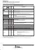
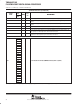
EMIF − CONTROL SIGNALS COMMON TO ALL TYPES OF MEMORY
#
CE3 V6 O/Z IPU
Memory space enables
CE2 W6 O/Z IPU
Memory space enables
• Enabled by bits 28 through 31 of the word address
CE1 W18 O/Z IPU
•
Enabled by bits 28 through 31 of the word address
•
Only one asserted during any external data access
CE0 V17 O/Z IPU
• Only one asserted during any external data access
BE1 U19 O/Z IPU
Byte-enable control
•
Decoded from the two lowest bits of the internal address
BE0 V20 O/Z IPU
• Decoded from the two lowest bits of the internal address
• Byte-write enables for most types of memory
• Can be directly connected to SDRAM read and write mask signal (SDQM)
EMIF − BUS ARBITRATION
#
HOLDA J18 O IPU Hold-request-acknowledge to the host
HOLD J17 I IPU Hold request from the host
BUSREQ J19 O IPU Bus request output
EMIF − ASYNCHRONOUS/SYNCHRONOUS DRAM/SYNCHRONOUS BURST SRAM MEMORY CONTROL
#
ECLKIN Y11 I IPD EMIF input clock
ECLKOUT Y10 O IPD
EMIF output clock depends on the EKSRC bit (DEVCFG.[4]) and on EKEN bit
(GBLCTL.[5])
EKSRC = 0 – ECLKOUT is based on the internal SYSCLK3 signal
from the clock generator (default).
EKSRC = 1 – ECLKOUT is based on the the external EMIF input clock
source pin (ECLKIN)
EKEN = 0 – ECLKOUT held low
EKEN = 1 – ECLKOUT enabled to clock (default)
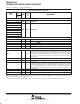
†
I = Input, O = Output, Z = High impedance, S = Supply voltage, GND = Ground, A = Analog signal (PLL Filter)
‡
IPD = Internal pulldown, IPU = Internal pullup. [To oppose the supply rail on these IPD/IPU signal pins, use external pullup or pulldown resistors
no greater than 4.4 kΩ and 2.0 kΩ, respectively.]
#
To maintain signal integrity for the EMIF signals, serial termination resistors should be inserted into all EMIF output signal lines.