
Floating Point Digital Signal Processor Specification Sheet

SPRS293A − OCTOBER 2005 − REVISED NOVEMBER 2005
62
POST OFFICE BOX 1443 • HOUSTON, TEXAS 77251−1443
electrical characteristics over recommended ranges of supply voltage and operating case
temperature
†
(unless otherwise noted)
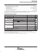
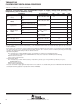
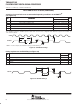
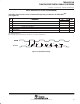
PARAMETER TEST CONDITIONS MIN TYP MAX UNIT
V
OH
High-level output
voltage
All signals except CLKS1 and
DR1
DV
DD
= MIN, I
OH
= MAX 2.4 V
V
OL
Low-level output
voltage
All signals except CLKS1 and
DR1
DV
DD
= MIN, I
OL
= MAX
0.4 V
V
OL
voltage
CLKS1 and DR1
DV
DD
= MIN, I
OL
= MAX
0.4 V
I
I
Input current
All signals except CLKS1 and
DR1
V
I
= V
SS
to DV
DD
±170 uA
I
I
Input current
CLKS1 and DR1
V
I
= V
SS
to DV
DD
±10 uA
I
OZ
Off-state output
current
All signals except CLKS1 and
DR1
V
O
= DV
DD
or 0 V
±170 uA
I
OZ
current
CLKS1 and DR1
V
O
= DV
DD
or 0 V
±10 uA
I
DD2V
Core supply current
‡
CV
DD
= 1.26 V, CPU
clock = 150 MHz
430 mA
I
DD3V
I/O supply current
‡
DV
DD
= 3.3 V,
EMIF speed = 100 MHz
75 mA
C
i
Input capacitance C6712D 7 pF
C
o
Output capacitance C6712D 7 pF
†
For test conditions shown as MIN, MAX, or NOM, use the appropriate value specified in the recommended operating conditions table.
‡
For more details on CPU, peripheral, and I/O activity, see the TMS320C62x/C67x Power Consumption Summary application report (literature
number SPRA486).
For the device, these currents were measured with average activity (50% high/50% low power) at 25°C case temperature and 100-MHz EMIF.
This model represents a device performing high-DSP-activity operations 50% of the time, and the remainder performing low-DSP-activity
operations. The high/low-DSP-activity models are defined as follows:
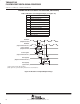
High-DSP-Activity Model:
CPU: 8 instructions/cycle with 2 LDDW instructions [L1 Data Memory: 128 bits/cycle via LDDW instructions;
L1 Program Memory: 256 bits/cycle; L2/EMIF EDMA: 50% writes, 50% reads to/from SDRAM (50% bit-switching)]
McBSP: 2 channels at E1 rate
Timers: 2 timers at maximum rate
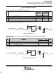
Low-DSP-Activity Model:
CPU: 2 instructions/cycle with 1 LDH instruction [L1 Data Memory: 16 bits/cycle; L1 Program Memory: 256 bits per 4 cycles;
L2/EMIF EDMA: None]
McBSP: 2 channels at E1 rate
Timers: 2 timers at maximum rate
The actual current draw is highly application-dependent. For more details on core and I/O activity, refer to the TMS320C6711D/12D/13B Power
Consumption Summary application report (literature number SPRA889A).