
Floating Point Digital Signal Processor Specification Sheet

SPRS293A − OCTOBER 2005 − REVISED NOVEMBER 2005
68
POST OFFICE BOX 1443 • HOUSTON, TEXAS 77251−1443
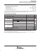
INPUT AND OUTPUT CLOCKS (CONTINUED)
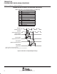
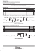
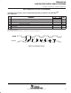
switching characteristics over recommended operating conditions for CLKOUT3
†‡
(see Figure 23)
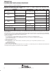
NO.
PARAMETER
−150
UNIT
NO.
PARAMETER
MIN MAX
UNIT
1 t
c(CKO3)
Cycle time, CLKOUT3 C3 − 0.9 C3 + 0.9 ns
2 t
w(CKO3H)
Pulse duration, CLKOUT3 high (C3/2) − 0.9 (C3/2) + 0.9 ns
3 t
w(CKO3L)
Pulse duration, CLKOUT3 low (C3/2) − 0.9 (C3/2) + 0.9 ns
4 t
t(CKO3)
Transition time, CLKOUT3 3 ns
5 t
d(CLKINH-CKO3V)
Delay time, CLKIN high to CLKOUT3 valid 1.5 7.5 ns
†
The reference points for the rise and fall transitions are measured at V
OL
MAX and V
OH
MIN.
‡
C3 = CLKOUT3 period in ns. CLKOUT3 period is a divide-down of the CPU clock, configurable via the OSCDIV1 register. For more details, see
PLL and PLL controller.
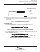
CLKIN
CLKOUT3
NOTE A: For this example, the CLKOUT3 frequency is CLKIN divide-by-2.
3
1
2
4
4
5
5
Figure 23. CLKOUT3 Timings
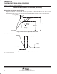
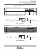
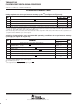
timing requirements for ECLKIN
§
(see Figure 24)
NO.
−150
UNIT
NO.
MIN MAX
UNIT
1 t
c(EKI)
Cycle time, ECLKIN 10 ns
2 t
w(EKIH)
Pulse duration, ECLKIN high 4.5 ns
3 t
w(EKIL)
Pulse duration, ECLKIN low 4.5 ns
4 t
t(EKI)
Transition time, ECLKIN 3 ns
§
The reference points for the rise and fall transitions are measured at V
IL
MAX and V
IH
MIN.
ECLKIN
1
2
3
4
4
Figure 24. ECLKIN Timings