
Floating Point Digital Signal Processor Specification Sheet


SPRS293A − OCTOBER 2005 − REVISED NOVEMBER 2005
9
POST OFFICE BOX 1443 • HOUSTON, TEXAS 77251−1443
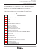
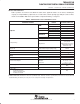
functional block and CPU (DSP core) diagram
Enhanced
DMA
Controller
(16 channel)
Test
C67x CPU (DSP Core)
Data Path B
B Register File
Instruction Fetch
Instruction Dispatch
Instruction Decode
Data Path A
A Register File
Power-Down
Logic
.L1
†
.S1
†
.M1
†
.D1 .D2 .M2
†
.S2
†
.L2
†
16
SDRAM
ROM/FLASH
SBSRAM
I/O Devices
L1P Cache
Direct Mapped
4K Bytes Total
Control
Registers
Control
Logic
In-Circuit
Emulation
Interrupt
Control
Framing Chips:
H.100, MVIP,
SCSA, T1, E1
AC97 Devices,
SPI Devices,
Codecs
Digital Signal Processor
†
In addition to fixed-point instructions, these functional units execute floating-point instructions.
‡
The device has a software-configurable PLL (with x4 through x25 multiplier and /1 through /32 divider) and a PLL Controller.
L2
Memory
4 Banks
64K Bytes
Total
PLL
‡
Timer 0
External
Memory
Interface
(EMIF)
Multichannel
Buffered
Serial Port 1
(McBSP1)
Multichannel
Buffered
Serial Port 0
(McBSP0)
SRAM
Timer 1
Interrupt
Selector
Boot
Configuration
GPIO
L1D Cache
2-Way Set
Associative
4K Bytes Total