
Stereo System User Manual


www.ti.com
4.18 Phase-Locked Loop (PLL)
4.18.1 PLL Device-Specific Information
1
0
PLLEN
(PLL_CSR[0])
Divider
D0
(/1 to /32)
PLLREF
PLL
x4 to x25
PLLOUT
Divider
D1
(/1 to /32)
SYSCLK1
CPU and Memory
Divider
D2
(/1 to /32)
SYSCLK2
Peripherals and dMAX
Divider
D3
(/1 to /32)
SYSCLK3
EMIF
AUXCLK
McASP0,1,2
Clock
Input
from
CLKIN or
OSCIN
TMS320C6727, TMS320C6726, TMS320C6722
Floating-Point Digital Signal Processors
SPRS268E – MAY 2005 – REVISED JANUARY 2007
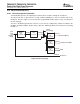
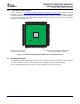
The C672x DSP generates the high-frequency internal clocks it requires through an on-chip PLL.
The input to the PLL is either from the on-chip oscillator (OSCIN pin) or from an external clock on the
CLKIN pin. The PLL outputs four clocks that have programmable divider options. Figure 4-43 illustrates
the PLL Topology.
The PLL is disabled by default after a device reset. It must be configured by software according to the
allowable operating conditions listed in Table 4-40 before enabling the DSP to run from the PLL by setting
PLLEN = 1.
Figure 4-43. PLL Topology
102 Peripheral and Electrical Specifications Submit Documentation Feedback