
Stereo System User Manual


www.ti.com
7 Mechanical Data
7.1 Package Thermal Resistance Characteristics
TMS320C6727, TMS320C6726, TMS320C6722
Floating-Point Digital Signal Processors
SPRS268E – MAY 2005 – REVISED JANUARY 2007
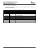
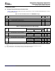
Table 7-1 and Table 7-2 provide the thermal characteristics for the recommended package types used on
the TMS320C672x DSP.
Table 7-1. Thermal Characteristics for GDH/ZDH Package
AIR FLOW
NO. ° C/W
(m/s)
Two-Signal, Two-Plane, 101.5 x 114.5 x 1.6 mm , 2-oz Cu. EIA/JESD51-9 PCB
1 R θ
JA
Thermal Resistance Junction to Ambient 25 0
2 R θ
JB
Thermal Resistance Junction to Board 14.5 0
3 R θ
JC
Thermal Resistance Junction to Top of Case 10 0
4 Ψ
JB
Thermal Metric Junction to Board 14 0
5 Ψ
JT
Thermal Metric Junction to Top of Case 0.39 0
Table 7-2. Thermal Characteristics for RFP Package
THERMAL PAD CONFIGURATION
AIR
NO. ° C/W FLOW
VIA
TOP BOTTOM
(m/s)
ARRAY
Two-Signal, Two-Plane, 76.2 x 76.2 mm PCB
(1) (2) (3)
1 R θ
JA
Thermal Resistance Junction to Ambient 10.6 x 10.6 mm 10.6 x 10.6 mm 6 x 6 20 0
7.5 x 7.5 mm 7.5 x 7.5 mm 5 x 5 22 0
2 Ψ
JP
Thermal Metric Junction to Power Pad 10.6 x 10.6 mm 10.6 x 10.6 mm 6 x 6 0.39 0
Double-Sided 76.2 x 76.2 mm PCB
(1) (2) (4)
3 R θ
JA
Thermal Resistance Junction to Ambient 10.6 x 10.6 mm 10.6 x 10.6 mm 6 x 6 49 0
10.6 x 10.6 mm 38.1 x 38.1 mm 6 x 6 27 0
10.6 x 10.6 mm 57.2 x 57 mm 6 x 6 22 0
10.6 x 10.6 mm 76.2 x 76.2 mm 6 x 6 20 0
4 Ψ
JP
Thermal Metric Junction to Power Pad 10.6 x 10.6 mm 10.6 x 10.6 mm 6 x 6 0.39 0
(1) PCB modeled with 2 oz/ft
2
Top and Bottom Cu.
(2) Package thermal pad must be properly soldered to top layer PCB thermal pad for both thermal and electrical performance. Thermal pad
is V
SS
.
(3) Top layer thermal pad is connected through via array to both bottom layer thermal pad and internal V
SS
plane.
(4) Top layer thermal pad is connected through via array to bottom layer thermal pad.
Submit Documentation Feedback Mechanical Data 107