
Stereo System User Manual


www.ti.com
4.5 Parameter Information
4.5.1 Parameter Information Device-Specific Information
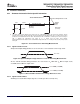
Transmission Line
4.0 pF 1.85 pF
Z0 = 50 Ω
(see note)
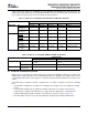
Tester Pin Electronics
Data Sheet Timing Reference Point
Output
Under
Test
42 Ω 3.5 nH
Device Pin
(see note)
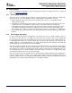
V
ref
= 1.5 V
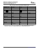
V
ref
= V
IL
MAX (or V
OL
MAX)
V
ref
= V
IH
MIN (or V
OH
MIN)
TMS320C6727, TMS320C6726, TMS320C6722
Floating-Point Digital Signal Processors
SPRS268E – MAY 2005 – REVISED JANUARY 2007
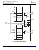
A. The data sheet provides timing at the device pin. For output timing analysis, the tester pin electronics and its
transmission line effects must be taken into account. A transmission line with a delay of 2 ns or longer can be used to
produce the desired transmission line effect. The transmission line is intended as a load only. It is not neccessary to
add or subtract the transmission line delay (2 ns or longer) from the data sheet timings.
Input requirements in this data sheet are tested with an input slew rate of < 4 Volts per nanosecond (4 V/ns) at the
device pin.
Figure 4-1. Test Load Circuit for AC Timing Measurements
4.5.1.1 Signal Transition Levels
All input and output timing parameters are referenced to 1.5 V for both "0" and "1" logic levels.
Figure 4-2. Input and Output Voltage Reference Levels for AC Timing Measurements
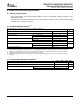
All rise and fall transition timing parameters are referenced to V
IL
MAX and V
IH
MIN for input clocks,
V
OL
MAX and V
OH
MIN for output clocks.
Figure 4-3. Rise and Fall Transition Time Voltage Reference Levels
4.5.1.2 Signal Transition Rates
All timings are tested with an input edge rate of 4 Volts per nanosecond (4 V/ns).
Submit Documentation Feedback Peripheral and Electrical Specifications 35