
Stereo System User Manual


www.ti.com
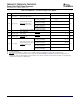
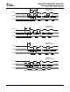
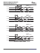
4.14.3 SPI Electrical Data/Timing
TMS320C6727, TMS320C6726, TMS320C6722
Floating-Point Digital Signal Processors
SPRS268E – MAY 2005 – REVISED JANUARY 2007
4.14.3.1 Serial Peripheral Interface (SPI) Timing
Table 4-25 through Table 4-32 assume testing over recommended operating conditions (see Figure 4-33
through Figure 4-36 ).
Table 4-25. General Timing Requirements for SPIx Master Modes
(1)
NO. MIN MAX UNIT
greater of 8P or
1 t
c(SPC)M
Cycle Time, SPIx_CLK, All Master Modes 256P ns
100 ns
2 t
w(SPCH)M
Pulse Width High, SPIx_CLK, All Master Modes greater of 4P or 45 ns ns
3 t
w(SPCL)M
Pulse Width Low, SPIx_CLK, All Master Modes greater of 4P or 45 ns ns
Polarity = 0, Phase = 0,
4P
to SPIx_CLK rising
Polarity = 0, Phase = 1,
0.5t
c(SPC)M
+ 4P
Delay, initial data bit valid
to SPIx_CLK rising
4 t
d(SIMO_SPC)M
on SPIx_SIMO to initial ns
Polarity = 1, Phase = 0,
edge on SPIx_CLK
(2)
4P
to SPIx_CLK falling
Polarity = 1, Phase = 1,
0.5t
c(SPC)M
+ 4P
to SPIx_CLK falling
Polarity = 0, Phase = 0,
15
from SPIx_CLK rising
Polarity = 0, Phase = 1,
15
Delay, subsequent bits
from SPIx_CLK falling
5 t
d(SPC_SIMO)M
valid on SPIx_SIMO after ns
Polarity = 1, Phase = 0,
transmit edge of SPIx_CLK
15
from SPIx_CLK falling
Polarity = 1, Phase = 1,
15
from SPIx_CLK rising
Polarity = 0, Phase = 0,
0.5t
c(SPC)M
– 10
from SPIx_CLK falling
Polarity = 0, Phase = 1,
Output hold time,
0.5t
c(SPC)M
– 10
from SPIx_CLK rising
SPIx_SIMO valid after
6 t
oh(SPC_SIMO)M
ns
receive edge of SPIxCLK,
Polarity = 1, Phase = 0,
0.5t
c(SPC)M
– 10
except for final bit
(3)
from SPIx_CLK rising
Polarity = 1, Phase = 1,
0.5t
c(SPC)M
– 10
from SPIx_CLK falling
Polarity = 0, Phase = 0,
0.5P + 15
to SPIx_CLK falling
Polarity = 0, Phase = 1,
0.5P + 15
Input Setup Time,
to SPIx_CLK rising
7 t
su(SOMI_SPC)M
SPIx_SOMI valid before ns
Polarity = 1, Phase = 0,
receive edge of SPIx_CLK
0.5P + 15
to SPIx_CLK rising
Polarity = 1, Phase = 1,
0.5P + 15
to SPIx_CLK falling
Polarity = 0, Phase = 0,
0.5P + 5
from SPIx_CLK falling
Polarity = 0, Phase = 1,
0.5P + 5
Input Hold Time,
from SPIx_CLK rising
8 t
ih(SPC_SOMI)M
SPIx_SOMI valid after ns
Polarity = 1, Phase = 0,
receive edge of SPIx_CLK
0.5P + 5
from SPIx_CLK rising
Polarity = 1, Phase = 1,
0.5P + 5
from SPIx_CLK falling
(1) P = SYSCLK2 period
(2) First bit may be MSB or LSB depending upon SPI configuration. MO(0) refers to first bit and MO(n) refers to last bit output on
SPIx_SIMO. MI(0) refers to the first bit input and MI(n) refers to the last bit input on SPIx_SOMI.
(3) The final data bit will be held on the SPIx_SIMO pin until the SPIDAT0 or SPIDAT1 register is written with new data.
Submit Documentation Feedback Peripheral and Electrical Specifications 83