
Stereo System User Manual


www.ti.com
TMS320C6727, TMS320C6726, TMS320C6722
Floating-Point Digital Signal Processors
SPRS268E – MAY 2005 – REVISED JANUARY 2007
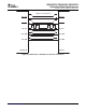
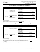
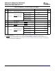
Table 4-30. Additional
(1)
SPI Slave Timings, 4-Pin Enable Option
(2) (3)
NO. MIN MAX UNIT
Polarity = 0, Phase = 0,
P – 10 3P + 15
from SPIx_CLK falling
Polarity = 0, Phase = 1,
0.5t
c(SPC)M
+ P – 10 0.5t
c(SPC)M
+ 3P + 15
Delay from final
from SPIx_CLK falling
24 t
d(SPC_ENAH)S
SPIx_CLK edge to slave ns
Polarity = 1, Phase = 0,
deasserting SPIx_ENA.
P – 10 3P + 15
from SPIx_CLK rising
Polarity = 1, Phase = 1,
0.5t
c(SPC)M
+ P – 10 0.5t
c(SPC)M
+ 3P + 15
from SPIx_CLK rising
(1) These parameters are in addition to the general timings for SPI slave modes (Table 4-26 ).
(2) P = SYSCLK2 period
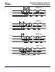
(3) Figure shows only Polarity = 0, Phase = 0 as an example. Table gives parameters for all four slave clocking modes.
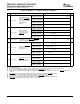
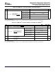
Table 4-31. Additional
(1)
SPI Slave Timings, 4-Pin Chip Select Option
(2) (3)
NO. MIN MAX UNIT
Required delay from SPIx_SCS asserted at slave to first
25 t
d(SCSL_SPC)S
P ns
SPIx_CLK edge at slave.
Polarity = 0, Phase = 0,
0.5t
c(SPC)M
+ P + 10
from SPIx_CLK falling
Polarity = 0, Phase = 1,
P + 10
Required delay from final
from SPIx_CLK falling
26 t
d(SPC_SCSH)S
SPIx_CLK edge before ns
Polarity = 1, Phase = 0,
SPIx_SCS is deasserted.
0.5t
c(SPC)M
+ P + 10
from SPIx_CLK rising
Polarity = 1, Phase = 1,
P + 10
from SPIx_CLK rising
Delay from master asserting SPIx_SCS to slave driving
27 t
ena(SCSL_SOMI)S
P + 15 ns
SPIx_SOMI valid
Delay from master deasserting SPIx_SCS to slave 3-stating
28 t
dis(SCSH_SOMI)S
P + 15 ns
SPIx_SOMI
(1) These parameters are in addition to the general timings for SPI slave modes (Table 4-26 ).
(2) P = SYSCLK2 period
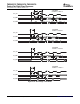
(3) Figure shows only Polarity = 0, Phase = 0 as an example. Table gives parameters for all four slave clocking modes.
Submit Documentation Feedback Peripheral and Electrical Specifications 87