
Digital Media System-on-Chip (DMSoC) Product Preview

www.ti.com
PRODUCT PREVIEW
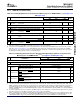
5.5.3 Clock PLL Electrical Data/Timing (Input and Output Clocks)
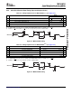
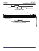
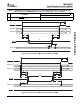
MXI/CLKIN
2
3
4
4
5
1
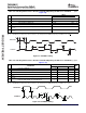
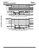
MXI/CLKIN
2
3
4
4
5
1
TMS320DM355
Digital Media System-on-Chip (DMSoC)
SPRS463A – SEPTEMBER 2007 – REVISED SEPTEMBER 2007
Table 5-5. Timing Requirements for MXI1/CLKIN1
(1) (2)
(see Figure 5-7 )
DM355
NO
UNIT
.
MIN TYP MAX
1 t
c(MXI1)
Cycle time, MXI1/CLKIN1 27. 7
(3)
41. 6
(3)
ns
2 t
w(MXI1H)
Pulse duration, MXI1/CLKIN1 high 0.45C 0.55C ns
3 t
w(MXI1L)
Pulse duration, MXI1/CLKIN1 low 0.45C 0.55C ns
4 t
t(MXI1)
Transition time, MXI1/CLKIN1 0.05C ns
5 t
J(MXI1)
Period jitter, MXI1/CLKIN1 0.02C ns
(1) The reference points for the rise and fall transitions are measured at V
IL
MAX and V
IH
MIN.
(2) C = MXI1/CLKIN1 cycle time in ns. For example, when MXI1/CLKIN1 frequency is 24 MHz use C = 41. 6 ns.
(3) tc(MXI1) = 41. 6 ns and tc(MXI1) = 27. 7 ns are the only supported cycle times for MXI1/CLKIN1.
Figure 5-7. MXI1/CLKIN1 Timing
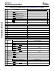
Table 5-6. Timing Requirements for MXI2/CLKIN2
(1) (2)
(see Figure 5-7 )
NO. DM355 UNIT
MIN TYP MAX
1 t
c(MXI2)
Cycle time, MXI2/CLKIN2 37. 037
(3)
37. 037
(3)
ns
2 t
w(MXI2H)
Pulse duration, MXI2/CLKIN2 high 0.45C 0.55C ns
3 t
w(MXI2L)
Pulse duration, MXI2/CLKIN2 low 0.45C 0.55C ns
4 t
t(MXI2)
Transition time, MXI2/CLKIN2 0.05C ns
5 t
J(MXI2)
Period jitter, MXI2/CLKIN2 0.02C ns
(1) The reference points for the rise and fall transitions are measured at V
IL
MAX and V
IH
MIN.
(2) C = MXI2/CLKIN2 cycle time in ns. For example, when MXI2/CLKIN2 frequency is 27 MHz use C = 37. 037 ns.
(3) tc(MXI2) = 37. 037 ns is the only supported cycle time for MXI2/CLKIN2.
Figure 5-8. MXI2/CLKIN2 Timing
Submit Documentation Feedback Peripheral Information and Electrical Specifications 101