
Digital Media System-on-Chip (DMSoC) Product Preview

www.ti.com
PRODUCT PREVIEW
TMS320DM355
Digital Media System-on-Chip (DMSoC)
SPRS463A – SEPTEMBER 2007 – REVISED SEPTEMBER 2007
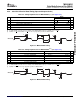
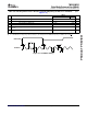
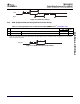
5.7.1.3 AEMIF Electrical Data/Timing
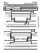
Table 5-13. Timing Requirements for Asynchronous Memory Cycles for AEMIF Module
(1)
(see Figure 5-14
and Figure 5-15 )
DM355
NO
UNIT
.
MIN Nom MAX
READS and WRITES
Pulse duration, EM_WAIT assertion and
2 t
w(EM_WAIT)
2E ns
deassertion
READS
12 t
su(EMDV-EMOEH)
Setup time, EM_D[15:0] valid before EM_OE high 5 ns
13 t
h(EMOEH-EMDIV)
Hold time, EM_D[15:0] valid after EM_OE high 0 ns
t
su(EMOEL-
Delay time from EM_OE low to EM_WAIT
14 4E ns
EMWAIT)
asserted
(2)
READS (OneNAND Synchronous Burst Read)
Setup time, EM_D[15:0] valid before EM_CLK
30 t
su(EMDV-EMCLKH)
4 ns
high
31 t
h(EMCLKH-EMDIV)
Hold time, EM_D[15:0] valid after EM_CLK high 4 ns
WRITES
t
su(EMWEL-
Delay time from EM_WE low to EM_WAIT
28 4E ns
EMWAIT)
asserted
(2)
(1) E = PLLC1 SYSCLK2 period in ns. SYSCLK2 is the EMIF peripheral clock. SYSCLK2 is one-fourth the PLLC output clock. For example,
when PLLC output clock = 432 MHz, E = 9.259 ns. See Section 3.5 for more information.
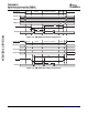
(2) Setup before end of STROBE phase (if no extended wait states are inserted) by which EM_WAIT must be asserted to add extended
wait states. Figure 5-16 and Figure 5-17 describe EMIF transactions that include extended wait states inserted during the STROBE
phase. However, cycles inserted as part of this extended wait period should not be counted; the 4E requirement is to the start of where
the HOLD phase would begin if there were no extended wait cycles.
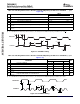
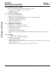
Table 5-14. Switching Characteristics Over Recommended Operating Conditions for Asynchronous
Memory Cycles for AEMIF Module
(1) (2) (3)
(see Figure 5-14 and Figure 5-15 )
DM355
UNI
NO. PARAMETER
T
MIN Nom MAX
READS and WRITES
1 t
d(TURNAROUND)
Turn around time (TA)*E ns
READS
EMIF read cycle time (EW = 0) (RS+RST+RH)*E ns
3 t
c(EMRCYCLE)
(RS+RST+RH+(EWC*
EMIF read cycle time (EW = 1) ns
16))*E
Output setup time, EM_CE[1:0] low to
(RS)*E ns
EM_OE low (SS = 0)
4 t
su(EMCEL-EMOEL)
Output setup time, EM_CE[1:0] low to
0 ns
EM_OE low (SS = 1)
Output hold time, EM_OE high to
(RH)*E ns
EM_CE[1:0] high (SS = 0)
5 t
h(EMOEH-EMCEH)
Output hold time, EM_OE high to
0 ns
EM_CE[1:0] high (SS = 1)
(1) TA = Turn around, RS = Read setup, RST = Read strobe, RH = Read hold, WS = Write setup, WST = Write strobe, WH = Write hold,
MEWC = Maximum external wait cycles. These parameters are programmed via the Asynchronous Bank and Asynchronous Wait Cycle
Configuration Registers. These support the following range of values: TA[4-1], RS[16-1], RST[64-1], RH[8-1], WS[16-1], WST[64-1],
WH[8-1], and MEW[1-256]. See the TMS320DM355 DMSoC Asynchronous External Memory Interface (EMIF) User's Guide (SPRUED1)
for more information.
(2) E = PLLC1 SYSCLK2 period in ns. SYSCLK2 is the EMIF peripheral clock. SYSCLK2 is one-fourth the PLLC output clock. For example,
when PLLC output clock = 432 MHz, E = 9.259 ns. See Section 3.5 for more information
(3) EWC = external wait cycles determined by EM_WAIT input signal. EWC supports the following range of values EWC[256-1]. Note that
the maximum wait time before timeout is specified by bit field MEWC in the Asynchronous Wait Cycle Configuration Register. See the
TMS320DM355 DMSoC Asynchronous External Memory Interface (EMIF) User's Guide (SPRUED1) for more information.
Submit Documentation Feedback Peripheral Information and Electrical Specifications 107