
Digital Media System-on-Chip (DMSoC) Product Preview

www.ti.com
PRODUCT PREVIEW
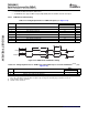
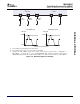
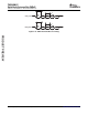
VCLK
(Positive Edge
Clocking)
VCLK
(Negative Edge
Clocking)
17
VCTL
(B)
VDATA
(C)
19
1822
21
23
24
25
26
VCLKIN
(A)
A. VCLKIN=PCLKorEXTCLK
B. VCTL=HSYNC,VSYNC,FIELD,andLCD_OE
C. VDATA=COUT[7:0],YOUT[7:0],R[7:3],G[7:2],andB[7:3]
20
20
TMS320DM355
Digital Media System-on-Chip (DMSoC)
SPRS463A – SEPTEMBER 2007 – REVISED SEPTEMBER 2007
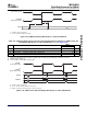
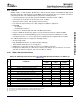
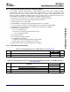
Table 5-24. Switching Characteristics Over Recommended Operating Conditions for VPBE Control and
Data Output With Respect to VCLK
(1) (2)
(see Figure 5-30 )
DM355
NO. PARAMETER UNIT
MIN MAX
17 t
c(VCLK)
Cycle time, VCLK 13.33 160 ns
18 t
w(VCLKH)
Pulse duration, VCLK high 5.7 ns
19 t
w(VCLKL)
Pulse duration, VCLK low 5.7 ns
20 t
t(VCLK)
Transition time, VCLK 3 ns
21 t
d(VCLKINH-VCLKH)
Delay time, VCLKIN high to VCLK high 2 12 ns
22 t
d(VCLKINL-VCLKL)
Delay time, VCLKIN low to VCLK low 2 12 ns
23 t
d(VCLK-VCTLV)
Delay time, VCLK edge to VCTL valid 4 ns
24 t
d(VCLK-VCTLIV)
Delay time, VCLK edge to VCTL invalid 0 ns
25 t
d(VCLK-VDATAV)
Delay time, VCLK edge to VDATA valid 4 ns
26 t
d(VCLK-VDATAIV)
Delay time, VCLK edge to VDATA invalid 0 ns
(1) The VPBE may be configured to operate in either positive or negative edge clocking mode. When in positive edge clocking mode, the
rising edge of VCLK is referenced. When in negative edge clocking mode, the falling edge of VCLK is referenced.
(2) VCLKIN = PCLK or EXTCLK. Note that if the CCDC is used, the PCLK frequency must be less than or equal to half the VPSS clock
frequency—i.e., PCLK ≤ SYSCLK4/2.
Figure 5-30. VPBE Control and Data Output Timing With Respect to VCLK
5.9.2.4 DAC and Video Buffer Electrical Data/Timing
The DAC and video buffer can be configured in a DAC only configuration or in a DAC and video buffer
configuration. In the DAC only configuration the internal video buffer is not used and an external video
buffer is attached to the DAC. In the DAC and video buffer configuration, the DAC and internal video
buffer are both used and a TV cable may be attached directly to the output of the video buffer. See
Figure 5-31 and Figure 5-32 for recommenced circuits for each configuration.
Peripheral Information and Electrical Specifications124 Submit Documentation Feedback