
Digital Media System-on-Chip (DMSoC) Product Preview


www.ti.com
PRODUCT PREVIEW
2.4 Pin Functions
2.4.1 Image Data Input - Video Processing Front End
TMS320DM355
Digital Media System-on-Chip (DMSoC)
SPRS463A – SEPTEMBER 2007 – REVISED SEPTEMBER 2007
The pin functions tables (Table 2-4 through Table 2-22 ) identify the external signal names, the associated
pin (ball) numbers along with the mechanical package designator, the pin type, whether the pin has any
internal pullup or pulldown resistors, and a functional pin description. For more detailed information on
device configuration, peripheral selection, multiplexed/shared pins, and debugging considerations, see
Section 3 . For the list of all pin in chronological order see Section 2.5
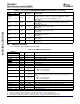
The CCD Controller module in the Video Processing Front End has an external signal interface for image
data input. It supports YUV (YC) inputs as well as Bayer RGB and complementary input signals (I.e.,
image data input).
The definition of the CCD controller data input signals depend on the input mode selected.
• In 16-bit YCbCr mode, the Cb and Cr signals are multiplexed on the Cl signals and the order is
configurable (i.e., Cb first or Cr first).
• In 8-bit YCbCr mode, the Y, Cb, and Cr signals are multiplexed and not only is the order selectable,
but also the half of the bus used.
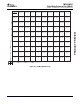
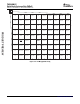
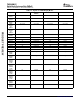
Table 2-4. CCD Controller Signals for Each Input Mode
PIN NAME CCD 16-BIT YCbCr 8-BIT YCbCr
Cl7 Cb7,Cr7 Y7,Cb7,Cr7
Cl6 Cb6,Cr6 Y6,Cb6,Cr6
Cl5 CCD13 Cb5,Cr5 Y5,Cb5,Cr5
Cl4 CCD12 Cb4,Cr4 Y4,Cb4,Cr4
Cl3 CCD11 Cb3,Cr3 Y3,Cb3,Cr3
Cl2 CCD10 Cb2,Cr2 Y2,Cb2,Cr2
Cl1 CCD9 Cb1,Cr1 Y1,Cb1,Cr1
Cl0 CCD8 Cb0,Cr0 Y0,Cb0,Cr0
Yl7 CCD7 Y7 Y7,Cb7,Cr7
Yl6 CCD6 Y6 Y6,Cb6,Cr6
Yl5 CCD5 Y5 Y5,Cb5,Cr5
Yl4 CCD4 Y4 Y4,Cb4,Cr4
Yl3 CCD3 Y3 Y3,Cb3,Cr3
Yl2 CCD2 Y2 Y2,Cb2,Cr2
Yl1 CCD1 Y1 Y1,Cb1,Cr1
Yl0 CCD0 Y0 Y0,Cb0,Cr0
Submit Documentation Feedback Device Overview 13