
Digital Media System-on-Chip (DMSoC) Product Preview


www.ti.com
PRODUCT PREVIEW
TMS320DM355
Digital Media System-on-Chip (DMSoC)
SPRS463A – SEPTEMBER 2007 – REVISED SEPTEMBER 2007
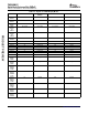
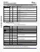
Table 2-5. CCD Controller/Video Input Terminal Functions
TERMINAL
TYPE
(1)
OTHER
(2) (3)
DESCRIPTION
NAME NO.
Standard CCD Analog Front End (AFE): NOT USED
• YCC 16-bit: Time multiplexed between chroma: CB/SR[07]
CIN7/
PD
• YCC 8-bit (which allows for two simultaneous decoder inputs), it is time
GIO101/ N3 I/O/Z
V
DD_VIN
multiplexed between luma and chroma of the upper channel. Y/CB/CR[07]
SPI2_SCLK
SPI: SPI2 Clock
GIO: GIO[101]
Standard CCD Analog Front End (AFE): NOT USED
• YCC 16-bit: Time multiplexed between chroma: CB/SR[06]
CIN6/
PD
• YCC 8-bit (which allows for two simultaneous decoder inputs), it is time
GIO100/ K5 I/O/Z
V
DD_VIN
multiplexed between luma and chroma of the upper channel. Y/CB/CR[06]
SPI2_SDO
SPI: SPI2 Data Out
GIO: GIO[100]
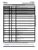
Standard CCD Analog Front End (AFE): Raw[13]
CIN5/ • YCC 16-bit: Time multiplexed between chroma: CB/SR[05]
GIO099/ PD
• YCC 8-bit (which allows for two simultaneous decoder inputs), it is time
M3 I/O/Z
SPI2_SDEN V
DD_VIN
multiplexed between luma and chroma of the upper channel. Y/CB/CR[05]
A[0]
SPI: SPI2 Chip Select
GIO: GIO[099]
Standard CCD Analog Front End (AFE): Raw[12]
CIN4/ • YCC 16-bit: Time multiplexed between chroma: CB/SR[04]
GIO098/ PD
• YCC 8-bit (which allows for two simultaneous decoder inputs), it is time
L4 I/O/Z
SPI2_SDEN V
DD_VIN
multiplexed between luma and chroma of the upper channel. Y/CB/CR[04]
A[1]
SPI: SPI2 Data In
GIO: GIO[098]
Standard CCD Analog Front End (AFE): Raw[11]
• YCC 16-bit: Time multiplexed between chroma: CB/SR[03]
CIN3/ PD
J4 I/O/Z
• YCC 8-bit (which allows for two simultaneous decoder inputs), it is time
GIO097/ V
DD_VIN
multiplexed between luma and chroma of the upper channel. Y/CB/CR[03]
GIO: GIO[097]
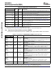
Standard CCD Analog Front End (AFE): Raw[10]
• YCC 16-bit: Time multiplexed between chroma: CB/SR[02]
CIN2/ PD
J5 I/O/Z
• YCC 8-bit (which allows for two simultaneous decoder inputs), it is time
GIO096/ V
DD_VIN
multiplexed between luma and chroma of the upper channel. Y/CB/CR[02]
GIO: GIO[097]
Standard CCD Analog Front End (AFE): Raw[09]
• YCC 16-bit: Time multiplexed between chroma: CB/SR[01]
CIN1/ PD
L3 I/O/Z
• YCC 8-bit (which allows for two simultaneous decoder inputs), it is time
GIO095/ V
DD_VIN
multiplexed between luma and chroma of the upper channel. Y/CB/CR[01]
GIO: GIO[095]
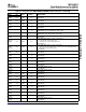
Standard CCD Analog Front End (AFE): Raw[08]
• YCC 16-bit: Time multiplexed between chroma: CB/SR[00]
CIN0/ PD
J3 I/O/Z
• YCC 8-bit (which allows for two simultaneous decoder inputs), it is time
GIO094/ V
DD_VIN
multiplexed between luma and chroma of the upper channel. Y/CB/CR[00]
GIO: GIO[094]
Standard CCD Analog Front End (AFE): Raw[07]
• YCC 16-bit: Time multiplexed between chroma: Y[07]
YIN7/ PD
L5 I/O/Z
• YCC 8-bit (which allows for two simultaneous decoder inputs), it is time
GIO093 V
DD_VIN
multiplexed between luma and chroma of the upper channel. Y/CB/CR[07]
GIO: GIO[093]
Standard CCD Analog Front End (AFE): Raw[06]
• YCC 16-bit: Time multiplexed between chroma: Y[06]
YIN6/ PD
M4 I/O/Z
• YCC 8-bit (which allows for two simultaneous decoder inputs), it is time
GIO092 V
DD_VIN
multiplexed between luma and chroma of the upper channel. Y/CB/CR[06]
GIO: GIO[092]
(1) I = Input, O = Output, Z = High impedance, S = Supply voltage, GND = Ground, A = Analog signal.
(2) PD = internal pull-down, PU = internal pull-up. (To pull up a signal to the opposite supply rail, a 1 k Ω resistor should be used.)
(3) Specifies the operating I/O supply voltage for each signal. See Section 5.3 , Power Supplies for more detail.
Device Overview14 Submit Documentation Feedback