
Digital Media System-on-Chip (DMSoC) Product Preview


www.ti.com
PRODUCT PREVIEW
2.4.3 Asynchronous External Memory Interface (AEMIF)
TMS320DM355
Digital Media System-on-Chip (DMSoC)
SPRS463A – SEPTEMBER 2007 – REVISED SEPTEMBER 2007
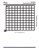
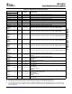
Table 2-8. Analog Video Terminal Functions
TERMINAL
TYPE
(1)
OTHER
(2)
DESCRIPTION
NAME NO.
Video DAC: Reference voltage output (0.45V, 0.1uF to GND). When the DAC is not
VREF J7 A I/O/Z
used, the VREF signal should be connected to V
SS
.
Video DAC: Pre video buffer DAC output (1000 ohm to VFB). When the DAC is not
IOUT E1 A I/O/Z
used, the IOUT signal should be connected to V
SS
.
Video DAC: External resistor (2550 Ohms to GND) connection for current bias
IBIAS F2 A I/O/Z configuration. When the DAC is not used, the IBIAS signal should be connected to
V
SS
.
Video DAC: Pre video buffer DAC output (1000 Ohms to IOUT, 1070 Ohms to
VFB G1 A I/O/Z
TVOUT). When the DAC is not used, the VFB signal should be connected to V
SS
.
Video DAC: Analog Composite NTSC/PAL output (SeeFigure 5-31 andFigure 5-32 for
TVOUT F1 A I/O/Z V circuit connection). When the DAC is not used, the TVOUT signal should be left as a
No Connect or connected to V
SS
.
Video DAC: Analog 1.8V power. When the DAC is not used, the V
DDA18_DAC
signal
V
DDA18_DAC
L7 PWR
should be connected to V
SS
.
Video DAC: Analog 1.8V ground. When the DAC is not used, the V
SSA_DAC
signal
V
SSA_DAC
L8 GND
should be connected to V
SS
.
(1) I = Input, O = Output, Z = High impedance, S = Supply voltage, GND = Ground, A = Analog signal. Specifies the operating I/O supply
voltage for each signal. See Section 5.3 , Power Supplies for more detail.
(2) PD = pull-down, PU = pull-up. (To pull up a signal to the opposite supply rail, a 1 k Ω resistor should be used.)
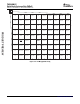
The Asynchronous External Memory Interface (AEMIF) signals support AEMIF, NAND, and OneNAND.
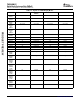
Table 2-9. Asynchronous EMIF/NAND/OneNAND Terminal Functions
TERMINAL
TYPE
(1)
OTHER
(2) (3)
DESCRIPTION
NAME NO.
Async EMIF: Address bus bit[13]
EM_A13/
PD GIO: GIO[67]
GIO067/ V19 I/O/Z
V
DD
System: BTSEL[1:0] sampled at power-on-reset to determine boot method. Used
BTSEL[1]
to drive boot status LED signal (active low) in ROM boot modes.
EM_A12/ Async EMIF: Address bus bit[12]
PD
GIO066/ U19 I/O/Z GIO: GIO[66]
V
DD
BTSEL[0] System: BTSEL[1:0] sampled at power-on-reset to determine boot method.
Async EMIF: Address bus bit[11]
EM_A11/
PU GIO: GIO[65]
GIO065/ R16 I/O/Z
V
DD
AECFG[3:0] sampled at power-on-reset to AECFG configuration. AECFG[3] sets
AECFG[3]
default for PinMux2_EM_D15_8: AEMIF default bus width (16 or 8 bits)
Async EMIF: Address bus bit[10]
EM_A10/ GIO: GIO[64]
PU
GIO064/ R18 I/O/Z AECFG[3:0] sampled at power-on-reset to AECFG configuration. AECFG[2:1]
V
DD
AECFG[2] sets default for PinMux2_EM_BA0: AEMIF EM_BA0 definition (EM_BA0,
EM_A14, GIO[054], rsvd)
Async EMIF: Address bus bit[09]
EM_A09/ GIO: GIO[63]
PD
GIO063/ P17 I/O/Z AECFG[3:0] sampled at power-on-reset to AECFG configuration. AECFG[2:1]
V
DD
AECFG[1] sets default for PinMux2_EM_BA0: AEMIF EM_BA0 definition (EM_BA0,
EM_A14, GIO[054], rsvd)
Async EMIF: Address bus bit[08]
GIO: GIO[62]
EM_A08/
PD
AECFG[0] sets default for:
GIO062/ T19 I/O/Z
V
DD
AECFG[0] • PinMux2_EM_A0_BA1: AEMIF address width (OneNAND or NAND)
• PinMux2_EM_A13_3: AEMIF address width (OneNAND or NAND)
EM_A07/ Async EMIF: Address bus bit[07]
P16 I/O/Z V
DD
GIO061 GIO: GIO[61]
(1) I = Input, O = Output, Z = High impedance, S = Supply voltage, GND = Ground, A = Analog signal.
(2) Specifies the operating I/O supply voltage for each signal. See Section 5.3 , Power Supplies for more detail.
(3) PD = pull-down, PU = pull-up. (To pull up a signal to the opposite supply rail, a 1 k Ω resistor should be used.)
Device Overview18 Submit Documentation Feedback