
Digital Media System-on-Chip (DMSoC) Product Preview


www.ti.com
PRODUCT PREVIEW
2.4.4 DDR Memory Interface
TMS320DM355
Digital Media System-on-Chip (DMSoC)
SPRS463A – SEPTEMBER 2007 – REVISED SEPTEMBER 2007
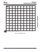
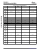
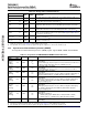
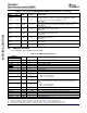
Table 2-9. Asynchronous EMIF/NAND/OneNAND Terminal Functions (continued)
TERMINAL
TYPE
(1)
OTHER
(2) (3)
DESCRIPTION
NAME NO.
Async EMIF: Lowest numbered chip select. Can be programmed to be used for
EM_CE0/ standard asynchronous memories (example: flash), OneNAND, or NAND
J16 I/O/Z V
DD
GIO037 memory. Used for the default boot and ROM boot modes.
GIO: GIO[037]
Async EMIF: Second chip select. Can be programmed to be used for standard
EM_CE1/
G19 I/O/Z V
DD
asynchronous memories(example: flash), OneNAND, or NAND memory.
GIO036
GIO: GIO[036]
Async EMIF: Write Enable
EM_WE/
J15 I/O/Z V
DD
NAND/SM/xD: WE (Write Enable) output
GIO035
GIO: GIO[035]
Async EMIF: Output Enable
EM_OE/
F19 I/O/Z V
DD
NAND/SM/xD: RE (Read Enable) output
GIO034
GIO: GIO[034]
Async EMIF: Async WAIT
EM_WAIT/
G18 I/O/Z V
DD
NAND/SM/xD: RDY/ BSY input
GIO033
GIO: GIO[033]
EM_ADV/ OneNAND: Address valid detect for OneNAND interface
H16 I/O/Z V
DD
GIO032 GIO: GIO[032]
EM_CLK/ OneNAND: Clock for OneNAND flash interface
E19 I/O/Z V
DD
GIO031 GIO: GIO[031]
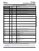
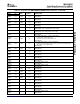
The DDR EMIF supports DDR2 and mobile DDR.
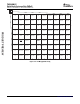
Table 2-10. DDR Terminal Functions
TERMINAL
TYPE
(1)
OTHER
(2) (3)
DESCRIPTION
NAME NO.
DDR_CLK W9 I/O/Z V
DD_DDR
DDR Data Clock
DDR_CLK W8 I/O/Z V
DD_DDR
DDR Complementary Data Clock
DDR_RAS T6 I/O/Z V
DD_DDR
DDR Row Address Strobe
DDR_CAS V9 I/O/Z V
DD_DDR
DDR Column Address Strobe
DDR_ WE W10 I/O/Z V
DD_DDR
DDR Write Enable
DDR_ CS T8 I/O/Z V
DD_DDR
DDR Chip Select
DDR_CKE V10 I/O/Z V
DD_DDR
DDR Clock Enable
DDR_DQM[
Data mask outputs:
U15 I/O/Z V
DD_DDR
1]
• DQM0 - For DDR_DQ[7:0]
DDR_DQM[
T12 I/O/Z V
DD_DDR
• DQM1 - For DDR_DQ[15:8]
0]
DDR_DQS[ Data strobe input/outputs for each byte of the 16-bit data bus used to
V15 I/O/Z V
DD_DDR
1] synchronize the data transfers. Output to DDR when writing and inputs when
reading.
DDR_DQS[
• DQS1 - For DDR_DQ[15:8]
V12 I/O/Z V
DD_DDR
0]
• DQS0 - For DDR_DQ[7:0]
DDR_BA[2] V8 I/O/Z V
DD_DDR
Bank select outputs. Two are required for 1Gb DDR2 memories.
DDR_BA[1] U7 I/O/Z V
DD_DDR
Bank select outputs. Two are required for 1Gb DDR2 memories.
DDR_BA[0] U8 I/O/Z V
DD_DDR
Bank select outputs. Two are required for 1Gb DDR2 memories.
DDR_A13 U6 I/O/Z V
DD_DDR
DDR Address Bus bit 13
DDR_A12 V7 I/O/Z V
DD_DDR
DDR Address Bus bit 12
DDR_A11 W7 I/O/Z V
DD_DDR
DDR Address Bus bit 11
(1) I = Input, O = Output, Z = High impedance, S = Supply voltage, GND = Ground, A = Analog signal.
(2) Specifies the operating I/O supply voltage for each signal. See Section 5.3 , Power Supplies for more detail.
(3) PD = pull-down, PU = pull-up. (To pull up a signal to the opposite supply rail, a 1 k Ω resistor should be used.)
Device Overview20 Submit Documentation Feedback