
Digital Media System-on-Chip (DMSoC) Product Preview

www.ti.com
PRODUCT PREVIEW
TMS320DM355
Digital Media System-on-Chip (DMSoC)
SPRS463A – SEPTEMBER 2007 – REVISED SEPTEMBER 2007
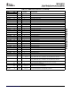
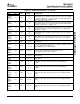
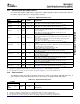
Table 2-10. DDR Terminal Functions (continued)
TERMINAL
TYPE
(1)
OTHER
(2) (3)
DESCRIPTION
NAME NO.
DDR_A10 V6 I/O/Z V
DD_DDR
DDR Address Bus bit 10
DDR_A09 W6 I/O/Z V
DD_DDR
DDR Address Bus bit 09
DDR_A08 W5 I/O/Z V
DD_DDR
DDR Address Bus bit 08
DDR_A07 V5 I/O/Z V
DD_DDR
DDR Address Bus bit 07
DDR_A06 U5 I/O/Z V
DD_DDR
DDR Address Bus bit 06
DDR_A05 W4 I/O/Z V
DD_DDR
DDR Address Bus bit 05
DDR_A04 V4 I/O/Z V
DD_DDR
DDR Address Bus bit 04
DDR_A03 W3 I/O/Z V
DD_DDR
DDR Address Bus bit 03
DDR_A02 W2 I/O/Z V
DD_DDR
DDR Address Bus bit 02
DDR_A01 V3 I/O/Z V
DD_DDR
DDR Address Bus bit 01
DDR_A00 V2 I/O/Z V
DD_DDR
DDR Address Bus bit 00
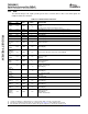
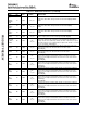
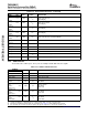
DDR_DQ15 W17 I/O/Z V
DD_DDR
DDR Data Bus bit 15
DDR_DQ14 V16 I/O/Z V
DD_DDR
DDR Data Bus bit 14
DDR_DQ13 W16 I/O/Z V
DD_DDR
DDR Data Bus bit 13
DDR_DQ12 U16 I/O/Z V
DD_DDR
DDR Data Bus bit 12
DDR_DQ11 W15 I/O/Z V
DD_DDR
DDR Data Bus bit 11
DDR_DQ10 W14 I/O/Z V
DD_DDR
DDR Data Bus bit 10
DDR_DQ09 V14 I/O/Z V
DD_DDR
DDR Data Bus bit 09
DDR_DQ08 U13 I/O/Z V
DD_DDR
DDR Data Bus bit 08
DDR_DQ07 W13 I/O/Z V
DD_DDR
DDR Data Bus bit 07
DDR_DQ06 V13 I/O/Z V
DD_DDR
DDR Data Bus bit 06
DDR_DQ05 W12 I/O/Z V
DD_DDR
DDR Data Bus bit 05
DDR_DQ04 U12 I/O/Z V
DD_DDR
DDR Data Bus bit 04
DDR_DQ03 T11 I/O/Z V
DD_DDR
DDR Data Bus bit 03
DDR_DQ02 U11 I/O/Z V
DD_DDR
DDR Data Bus bit 02
DDR_DQ01 W11 I/O/Z V
DD_DDR
DDR Data Bus bit 01
DDR_DQ00 V11 I/O/Z V
DD_DDR
DDR Data Bus bit 00
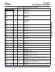
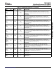
DDR_GATE DDR: Loopback signal for external DQS gating. Route to DDR and back to
W18 I/O/Z V
DD_DDR
0 DDR_GATE0 with same constraints as used for DDR clock and data.
DDR_GATE DDR: Loopback signal for external DQS gating. Route to DDR and back to
V17 I/O/Z V
DD_DDR
1 DDR_GATE0 with same constraints as used for DDR clock and data.
DDR: Voltage input for the SSTL_18 I/O buffers. Note even in the case of mDDR
DDR_VREF U10 I/O/Z V
DD_DDR
an external resistor divider connected to this pin is necessary.
V
SSA_DLL
R11 I/O/Z V
DD_DDR
DDR: Ground for the DDR DLL
V
DDA33_DDR
R10 I/O/Z V
DD_DDR
DDR: Power (3.3 V) for the DDR DLL
DLL
DDR: Reference output for drive strength calibration of N and P channel outputs.
DDR_ZN T9 I/O/Z V
DD_DDR
Tie to ground via 50 ohm resistor @ 0.5% tolerance.
Submit Documentation Feedback Device Overview 21