
Digital Media System-on-Chip (DMSoC) Product Preview

www.ti.com
PRODUCT PREVIEW
2.4.15 System Configuration Interface
TMS320DM355
Digital Media System-on-Chip (DMSoC)
SPRS463A – SEPTEMBER 2007 – REVISED SEPTEMBER 2007
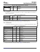
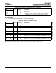
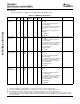
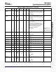
Table 2-20. PWM Terminal Functions (continued)
TERMINAL
TYPE
(1)
OTHER
(2) (3)
DESCRIPTION
NAME NO.
COUT3-
B6 / Digital Video Out: VENC settings determine function GIO: GIO[077]
GIO077 / E3 I/O/Z V
DD_VOUT
PWM2C
PWM2C / RTO2
RTO2
COUT2-
B5 / Digital Video Out: VENC settings determine function GIO: GIO[076]
GIO076 / E4 I/O/Z V
DD_VOUT
PWM2D
PWM2D / RTO3
RTO3
COUT1-
B4 / Digital Video Out: VENC settings determine function GIO: GIO[075]
F3 I/O/Z V
DD_VOUT
GIO075 / PWM3A
PWM3A
COUT0-
B3 / Digital Video Out: VENC settings determine function GIO: GIO[074]
F4 I/O/Z V
DD_VOUT
GIO074 / PWM3B
PWM3B
FIELD /
Video Encoder: Field identifier for interlaced display formats GIO: GIO[070]
GIO070 /
H4 I/O/Z V
DD_VOUT
Digital Video Out: R2
R2 /
PWM3C
PWM3C
EXTCLK /
Video Encoder: External clock input, used if clock rates > 27 MHz are needed,
GIO069 / PD
G3 I/O/Z e.g. 74.25 MHz for HDTV digital output GIO: GIO[069] Digital Video Out: B2
B2 / V
DD_VOUT
PWM3D
PWM3D
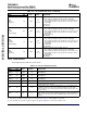
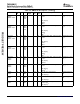
The provides interfaces for system configuration and boot load.
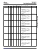
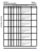
Table 2-21. System/Boot Terminal Functions
TERMINAL
TYPE
(1)
OTHER
(2) (3)
DESCRIPTION
NAME NO.
Async EMIF: Address bus bit 13
EM_A13/
PD GIO: GIO[067]
GIO067/ V19 I/O/Z
V
DD
System: BTSEL[1:0] sampled at power-on-reset to determine boot method. Used
BTSEL[1]
to drive boot status LED signal (active low) in ROM boot modes.
EM_A12/ Async EMIF: Address bus bit 12
PD
GIO066/ U19 I/O/Z GIO: GIO[066]
V
DD
BTSEL[0] System: BTSEL[1:0] sampled at power-on-reset to determine boot method.
Async EMIF: Address bus bit 11
EM_A11/ GIO: GIO[065]
PU
GIO065/ R16 I/O/Z System: AECFG[3:0] sampled a power-on-reset to set AEMIF configuration.
V
DD
AECFG[3] AECFG[3] sets default fo PinMux2.EM_D15_8. AEMIF default bus width (16 or 8
bits).
Async EMIF: Address bus bit 10
EM_A10/ GIO: GIO[064]
PU
GIO064/ R18 I/O/Z System: AECFG[3:0] sampled a power-on-reset to set AEMIF configuration.
V
DD
AECFG[2] AECFG[2:1] sets default fo PinMux2.EM_BA0. AEMIF EM_BA0 definition:
(EM,_BA0, EM_A14, GOP[054], rsvd)
Async EMIF: Address bus bit 09
EM_A09/ GIO: GIO[063]
PD
GIO063/ P17 I/O/Z System: AECFG[3:0] sampled a power-on-reset to set AEMIF configuration.
V
DD
AECFG[1] AECFG[2:1] sets default fo PinMux2.EM_BA0. AEMIF EM_BA0 definition:
(EM,_BA0, EM_A14, GOP[054], rsvd)
(1) I = Input, O = Output, Z = High impedance, S = Supply voltage, GND = Ground, A = Analog signal.
(2) Specifies the operating I/O supply voltage for each signal. See Section 5.3 , Power Supplies for more detail.
(3) PD = pull-down, PU = pull-up. (To pull up a signal to the opposite supply rail, a 1 k Ω resistor should be used.)
Device Overview34 Submit Documentation Feedback