
Digital Media System-on-Chip (DMSoC) Product Preview

www.ti.com
PRODUCT PREVIEW
2.5 Pin List
TMS320DM355
Digital Media System-on-Chip (DMSoC)
SPRS463A – SEPTEMBER 2007 – REVISED SEPTEMBER 2007
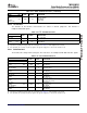
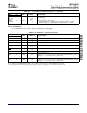
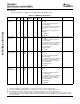
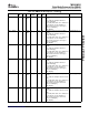
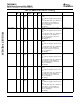
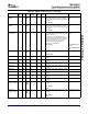
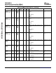
Table 2-23 provides a complete pin description list in pin number order.
Table 2-23. DM355 Pin Descriptions
Name BGA Type Group Power PU Reset Description
(4)
Mux Control
ID
(1)
Supply
(2)
PD
(3)
State
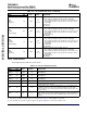
CIN7 / GIO101 / N3 I/O CCDC V
DD_VIN
PD in Standard CCD Analog Front End (AFE): PINMUX0[1:0].CIN_
SPI2_SCLK / GIO / NOT USED 7
SPI2
YCC 16-bit: time multiplexed between
chroma: CB/CR[07]
YCC 08-bit (which allows for 2 simultaneous
decoder inputs), it is time multiplexed
between
luma and chroma of the upper channel.
Y/CB/CR[07]
SPI: SPI2 Clock
GIO: GIO[101]
CIN6 / GIO100 / K5 I/O CCDC V
DD_VIN
PD in Standard CCD Analog Front End (AFE): PINMUX0[3:2].CIN_
SPI2_SDO / GIO / NOT USED 6
SPI2
YCC 16-bit: time multiplexed between
chroma: CB/CR[06]
YCC 08-bit (which allows for 2 simultaneous
decoder inputs), it is time multiplexed
between luma and chroma of the upper
channel. Y/CB/CR[06]
SPI: SPI2 Data Out
GIO: GIO[100]
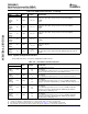
CIN5 / GIO099 / M3 I/O CCDC V
DD_VIN
PD in Standard CCD Analog Front End (AFE): PINMUX0[5:4].CIN_
SPI2_SDENA[0] / GIO / raw[13] 5
SPI2
YCC 16-bit: time multiplexed between
chroma: CB/CR[05]
YCC 08-bit (which allows for 2 simultaneous
decoder inputs), it is time multiplexed
between luma and chroma of the upper
channel. Y/CB/CR[05]
SPI: SPI2 Chip Select
GIO: GIO[99]
CIN4 / GIO098 / L4 I/O CCDC V
DD_VIN
PD in Standard CCD Analog Front End (AFE): PINMUX0[7:6].CIN_
SPI2_SDI / / GIO / raw[12] 4
SPI2_SDENA[1] SPI2 /
SPI2
YCC 16-bit: time multiplexed between
chroma: CB/CR[04]
YCC 08-bit (which allows for 2 simultaneous
decoder inputs), it is time multiplexed
between luma and chroma of the upper
channel. Y/CB/CR[04]
SPI: SPI2 Data In
GIO: GIO[098]
(1) I = Input, O = Output, Z = High impedance, S = Supply voltage, GND = Ground, A = Analog signal.
(2) Specifies the operating I/O supply voltage for each signal. See Section 5.3 , Power Supplies for more detail.
(3) PD = pull-down, PU = pull-up. (To pull up a signal to the opposite supply rail, a 1 k Ω resistor should be used.)
(4) To reduce EMI and reflections, depending on the trace length, approximately 22 Ω to 50 Ω damping resistors are recommend on the
following outputs placed near the DM355: YOUT(0-7),COUT(0-7), HSYNC,VSYNC,LCD_OE,FIELD,EXTCLK,VCLK. The trace lengths
should be minimized.
Device Overview36 Submit Documentation Feedback