
Digital Media System-on-Chip (DMSoC) Product Preview

www.ti.com
PRODUCT PREVIEW
TMS320DM355
Digital Media System-on-Chip (DMSoC)
SPRS463A – SEPTEMBER 2007 – REVISED SEPTEMBER 2007
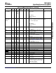
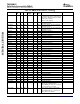
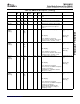
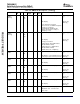
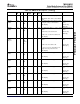
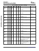
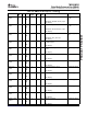
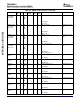
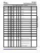
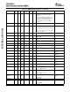
Table 2-23. DM355 Pin Descriptions (continued)
Name BGA Type Group Power PU Reset Description
(4)
Mux Control
ID
(1)
Supply
(2)
PD
(3)
State
FIELD / GIO070 H4 I/O VENC V
DD_VOUT
in Video Encoder: Field identifier for interlaced PINMUX1[19:18].FI
/ R2 / PWM3C / GIO / display formats ELD
VENC
/
PWM3
GIO: GIO[070]
Digital Video Out: R2
PWM3C
(4)
EXTCLK / G3 I/O VENC V
DD_VOUT
PD in Video Encoder: External clock input, used if PINMUX1[21:20].EX
GIO069 / B2 / / GIO / clock rates > 27 MHz are needed, e.g. 74.25 TCLK
PWM3D VENC MHz for HDTV digital output
/
PWM3
GIO: GIO[069]
Digital Video Out: B2
PWM3D
(4)
VCLK / GIO068 H3 I/O VENC V
DD_VOUT
out L Video Encoder: Video Output Clock PINMUX1[22].VCLK
/ GIO
GIO: GIO[068]
(4)
VREF J7 A I/O Video Video DAC: Reference voltage output
DAC (0.45V, 0.1uF to GND)
IOUT E1 A I/O Video Video DAC: Pre video buffer DAC output
DAC (1000 ohm to VFB)
IBIAS F2 A I/O Video Video DAC: External resistor (2550 Ohms to
DAC GND) connection for current bias
configuration
VFB G1 A I/O Video Video DAC: Pre video buffer DAC output
DAC (1000 ohm to IOUT, 1070 ohm to TVOUT)
TVOUT F1 A I/O Video V
DDA18_DAC
Video DAC: Analog Composite NTSC/PAL
DAC output (SeeFigure 5-31 andFigure 5-32 for
circuit connection)
V
DDA18V_DAC
L7 PWR Video Video DAC: Analog 1.8V power
DAC
V
SSA_DAC
L8 GND Video Video DAC: Analog 1.8V ground
DAC
DDR_CLK W9 I/O DDR V
DD_DDR
out L DDR Data Clock
DDR_CLK W8 I/O DDR V
DD_DDR
out H DDR Complementary Data Clock
DDR_RAS T6 I/O DDR V
DD_DDR
out H DDR Row Address Strobe
DDR_CAS V9 I/O DDR V
DD_DDR
out H DDR Column Address Strobe
DDR_WE W10 I/O DDR V
DD_DDR
out H DDR Write Enable (active low)
DDR_CS T8 I/O DDR V
DD_DDR
out H DDR Chip Select (active low)
DDR_CKE V10 I/O DDR V
DD_DDR
out L DDR Clock Enable
DDR_DQM[1] U15 I/O DDR V
DD_DDR
out L Data mask outputs: DQM0: For
DDR_DQ[7:0]
DDR_DQM[0] T12 I/O DDR V
DD_DDR
out L Data mask outputs: DQM1: For
DDR_DQ[15:8]
DDR_DQS[1] V15 I/O DDR V
DD_DDR
in Data strobe input/outputs for each byte of
the 16 bit data bus used to synchronize the
data transfers. Output to DDR when writing
and inputs when reading.
DQS1: For DDR_DQ[15:8]
Submit Documentation Feedback Device Overview 41