
Digital Media System-on-Chip (DMSoC) Product Preview

www.ti.com
PRODUCT PREVIEW
TMS320DM355
Digital Media System-on-Chip (DMSoC)
SPRS463A – SEPTEMBER 2007 – REVISED SEPTEMBER 2007
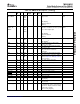
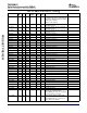
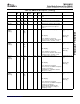
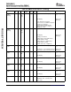
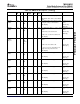
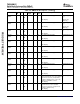
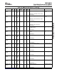
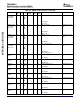
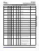
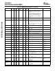
Table 2-23. DM355 Pin Descriptions (continued)
Name BGA Type Group Power PU Reset Description
(4)
Mux Control
ID
(1)
Supply
(2)
PD
(3)
State
DDR_DQS[0] V12 I/O DDR V
DD_DDR
in Data strobe input/outputs for each byte of
the 16 bit data bus used to synchronize the
data transfers. Output to DDR when writing
and inputs when reading.
DQS0: For DDR_DQ[7:0]
DDR_BA[2] V8 I/O DDR V
DD_DDR
out L Bank select outputs. Two are required for
1Gb DDR2 memories.
DDR_BA[1] U7 I/O DDR V
DD_DDR
out L Bank select outputs. Two are required for
1Gb DDR2 memories.
DDR_BA[0] U8 I/O DDR V
DD_DDR
out L Bank select outputs. Two are required for
1Gb DDR2 memories.
DDR_A13 U6 I/O DDR V
DD_DDR
out L DDR Address Bus bit 13
DDR_A12 V7 I/O DDR V
DD_DDR
out L DDR Address Bus bit 12
DDR_A11 W7 I/O DDR V
DD_DDR
out L DDR Address Bus bit 11
DDR_A10 V6 I/O DDR V
DD_DDR
out L DDR Address Bus bit 10
DDR_A09 W6 I/O DDR V
DD_DDR
out L DDR Address Bus bit 09
DDR_A08 W5 I/O DDR V
DD_DDR
out L DDR Address Bus bit 08
DDR_A07 V5 I/O DDR V
DD_DDR
out L DDR Address Bus bit 07
DDR_A06 U5 I/O DDR V
DD_DDR
out L DDR Address Bus bit 06
DDR_A05 W4 I/O DDR V
DD_DDR
out L DDR Address Bus bit 05
DDR_A04 V4 I/O DDR V
DD_DDR
out L DDR Address Bus bit 04
DDR_A03 W3 I/O DDR V
DD_DDR
out L DDR Address Bus bit 03
DDR_A02 W2 I/O DDR V
DD_DDR
out L DDR Address Bus bit 02
DDR_A01 V3 I/O DDR V
DD_DDR
out L DDR Address Bus bit 01
DDR_A00 V2 I/O DDR V
DD_DDR
out L DDR Address Bus bit 00
DDR_DQ15 W17 I/O DDR V
DD_DDR
in DDR Data Bus bit 15
DDR_DQ14 V16 I/O DDR V
DD_DDR
in DDR Data Bus bit 14
DDR_DQ13 W16 I/O DDR V
DD_DDR
in DDR Data Bus bit 13
DDR_DQ12 U16 I/O DDR V
DD_DDR
in DDR Data Bus bit 12
DDR_DQ11 W15 I/O DDR V
DD_DDR
in DDR Data Bus bit 11
DDR_DQ10 W14 I/O DDR V
DD_DDR
in DDR Data Bus bit 10
DDR_DQ09 V14 I/O DDR V
DD_DDR
in DDR Data Bus bit 09
DDR_DQ08 U13 I/O DDR V
DD_DDR
in DDR Data Bus bit 08
DDR_DQ07 W13 I/O DDR V
DD_DDR
in DDR Data Bus bit 07
DDR_DQ06 V13 I/O DDR V
DD_DDR
in DDR Data Bus bit 06
DDR_DQ05 W12 I/O DDR V
DD_DDR
in DDR Data Bus bit 05
DDR_DQ04 U12 I/O DDR V
DD_DDR
in DDR Data Bus bit 04
DDR_DQ03 T11 I/O DDR V
DD_DDR
in DDR Data Bus bit 03
DDR_DQ02 U11 I/O DDR V
DD_DDR
in DDR Data Bus bit 02
DDR_DQ01 W11 I/O DDR V
DD_DDR
in DDR Data Bus bit 01
DDR_DQ00 V11 I/O DDR V
DD_DDR
in DDR Data Bus bit 00
DDR_GATE0 W18 I/O DDR V
DD_DDR
DDR: Loopback signal for external DQS
gating. Route to DDR and back to
DDR_STRBEN_DEL with same constraints
as used for DDR clock and data.
DDR_GATE1 V17 I/O DDR V
DD_DDR
DDR: Loopback signal for external DQS
gating. Route to DDR and back to
DDR_STRBEN with same constraints as
used for DDR clock and data.
Device Overview42 Submit Documentation Feedback