
Digital Media System-on-Chip (DMSoC) Product Preview

www.ti.com
PRODUCT PREVIEW
TMS320DM355
Digital Media System-on-Chip (DMSoC)
SPRS463A – SEPTEMBER 2007 – REVISED SEPTEMBER 2007
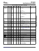
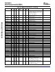
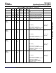
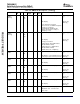
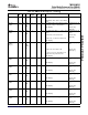
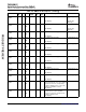
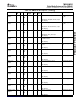
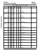
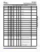
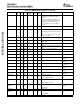
Table 2-23. DM355 Pin Descriptions (continued)
Name BGA Type Group Power PU Reset Description
(4)
Mux Control
ID
(1)
Supply
(2)
PD
(3)
State
SPI1_SCLK / C13 I/O SPI1 / V
DD
in SPI1: Clock PINMUX3[24].GIO1
GIO010 GIO 0
GIO: GIO[010]
SPI1_SDI / A13 I/O SPI1 / V
DD
in SPI1: Data In -OR- SPI1: Chip Select 1 PINMUX3[26:25].GI
GIO009 / GIO / O9
SPI1_SDENA[1] SPI1
GIO: GIO[009]
SPI1_SDO / E12 I/O SPI1 / V
DD
in SPI1: Data Out PINMUX3[27].GIO8
GIO008 GIO
GIO: GIO[008]
GIO007 / C17 I/O GIO V
DD
in GIO: GIO[007] PINMUX3[28].GIO7
SPI0_SDENA[1] debou
nce /
SPI0
SPI0: Chip Select 1
GIO006 B18 I/O GIO V
DD
in GIO: GIO[006]
debou
nce
GIO005 D15 I/O GIO V
DD
in GIO: GIO[005]
debou
nce
GIO004 B17 I/O GIO V
DD
in GIO: GIO[004]
debou
nce
GIO003 G15 I/O GIO V
DD
in GIO: GIO[003]
debou
nce
GIO002 F15 I/O GIO V
DD
in GIO: GIO[002]
debou
nce
GIO001 E14 I/O GIO V
DD
in GIO: GIO[001]
debou
nce
GIO000 C16 I/O GIO V
DD
in GIO: GIO[000]
debou
nce
USB_DP A7 A I/O USBP V
DDA33_USB
USB D+ (differential signal pair)
HY
USB_DM A6 A I/O USBP V
DDA33_USB
USB D- (differential signal pair)
HY
USB_R1 C7 A I/O USBP USB Reference current output
HY
Connect to V
SS_USB_REF
via 10K Ω ± 1%
resistor placed as close to the device as
possible.
USB_ID D5 A I/O USBP V
DDA33_USB
USB operating mode identification pin
HY
For Device mode operation only, pull up this
pin to VDD with a 1.5K ohm resistor.
For Host mode operation only, pull down this
pin to ground (VSS) with a 1.5K ohm
resistor.
If using an OTG or mini-USB connector, this
pin will be set properly via the
cable/connector configuration.
Submit Documentation Feedback Device Overview 49