
Digital Media System-on-Chip (DMSoC) Product Preview


www.ti.com
PRODUCT PREVIEW
3.5.4 Peripheral Clocking Considerations
TMS320DM355
Digital Media System-on-Chip (DMSoC)
SPRS463A – SEPTEMBER 2007 – REVISED SEPTEMBER 2007
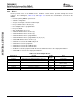
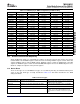
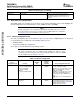
3.5.3.2.2 DM355-270 PLL2 (36 MHz reference)
All supported clocking configurations for DM355-270 PLL2 with 36 MHz reference clock are shown in
Table 3-5
Table 3-9. PLL2 Supported Clocking Configurations for DM355-270 (36 MHz reference)
PREDIV PLLM POSTDIV PLL2 VCO DDR PHY DDR Clock
(/n programmable) (m (/1 fixed) (MHz) PLLDIV1 SYSCLK1 DDR_CLK
programmable) (/1 fixed) (MHz) (MHz)
bypass bypass bypass bypass 1 36 18
12 144 1 432 1 432 216
12 138 1 414 1 414 207
12 132 1 396 1 396 198
12 126 1 378 1 378 189
12 120 1 360 1 360 180
12 114 1 342 1 342 171
12 108 1 324 1 324 162
12 102 1 306 1 306 153
12 96 1 288 1 288 144
18 133 1 266 1 266 133
27 150 1 200 1 200 100
27 120 1 160 1 160 80
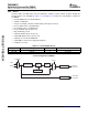
3.5.4.1 Video Processing Back End Clocking
The Video Processing Back End (VPBE) is a sub-module of the VPSS (Video Processing Subsystem).
The VPBE is designed to interface with a variety of LCDs and an internal DAC module. There are two
asynchronous clock domains in the VPBE: an internal clock domain and an external clock domain. The
internal clock domain is driven by the VPSS clock (PLL1 SYSCLK4). The external clock domain is
configurable; you can select one of five source:
• 24 MHz crystal input at MXI1
• 27 MHz crystal input at MXI2 (optional feature, not typically used)
• PLL1 SYSCLK3
• EXTCLK pin (external VPBE clock input pin)
• PCLK pin (VPFE pixel clock input pin)
See the TMS320DM355 DMSoC Video Processing Back End (VPBE) User's Guide for complete
information on VPBE clocking.
3.5.4.2 USB Clocking
The USB Controller is driven by two clocks: an output clock of PLL1 (SYSCLK2) and an output clock of
the USB PHY.
NOTE
For proper USB function, SYSCLK2 must be greater than 60 MHz.
The USB PHY takes an input clock that is configurable by the USB PHY clock source bits (PHYCLKSRC)
in the USB PHY control register (USB_PHY_CTL) in the System Control Module. When a 24 MHz crystal
is used at MXI1/MXO1, set PHYCLKSRC to 0. This will present a 24 MHz clock to the USB PHY. When a
36 MHz crystal is used at MXI1/MXO1, set PHYCLKSRC to 1. This will present a 12 MHz clock (36 MHz
Submit Documentation Feedback Detailed Device Description 71