
Digital Media System-on-Chip (DMSoC) Product Preview


www.ti.com
PRODUCT PREVIEW
3.9.2 Software Controlled Pin Multiplexing
3.10 Device Reset
TMS320DM355
Digital Media System-on-Chip (DMSoC)
SPRS463A – SEPTEMBER 2007 – REVISED SEPTEMBER 2007
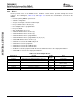
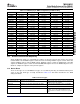
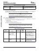
Table 3-13. AECFG (Async EMIF Configuration) Pin Mux Coding
1101(NAND) 1100 1010 (OneNAND) 1000 (8-bit SRAM) 0010 (16-bit SRAM) 0000
GPIO[54] GPIO[54] EM_A[14] EM_BA[0] EM_A[14] EM_BA[0]
GPIO[55] EM_BA[1] EM_BA[1] EM_BA[1] EM_BA[1] EM_BA[1]
GPIO[56] EM_A[0] EM_A[0] EM_A[0] EM_A[0] EM_A[0]
EM_A[1] EM_A[1] EM_A[1] EM_A[1] EM_A[1] EM_A[1]
EM_A[2] EM_A[2] EM_A[2] EM_A[2] EM_A[2] EM_A[2]
GPIO[57] EM_A[3] EM_A[3] EM_A[3] EM_A[3] EM_A[3]
GPIO[58] EM_A[4] EM_A[4] EM_A[4] EM_A[4] EM_A[4]
GPIO[59] EM_A[5] EM_A[5] EM_A[5] EM_A[5] EM_A[5]
GPIO[60] EM_A[6] EM_A[6] EM_A[6] EM_A[6] EM_A[6]
GPIO[61] EM_A[7] EM_A[7] EM_A[7] EM_A[7] EM_A[7]
GPIO[62] EM_A[8] EM_A[8] EM_A[8] EM_A[8] EM_A[8]
GPIO[63] EM_A[9] EM_A[9] EM_A[9] EM_A[9] EM_A[9]
GPIO[64] EM_A[10] EM_A[10] EM_A[10] EM_A[10] EM_A[10]
GPIO[65] EM_A[11] EM_A[11] EM_A[11] EM_A[11] EM_A[11]
GPIO[66] EM_A[12] EM_A[12] EM_A[12] EM_A[12] EM_A[12]
GPIO[67] EM_A[13] EM_A[13] EM_A[13] EM_A[13] EM_A[13]
GPIO[46] GPIO[46] GPIO[46] GPIO[46] EM_D[8] EM_D[8]
GPIO[47] GPIO[47] GPIO[47] GPIO[47] EM_D[9] EM_D[9]
GPIO[48] GPIO[48] GPIO[48] GPIO[48] EM_D[10] EM_D[10]
GPIO[49] GPIO[49] GPIO[49] GPIO[49] EM_D[11] EM_D[11]
GPIO[50] GPIO[50] GPIO[50] GPIO[50] EM_D[12] EM_D[12]
GPIO[51] GPIO[51] GPIO[51] GPIO[51] EM_D[13] EM_D[13]
GPIO[52] GPIO[52] GPIO[52] GPIO[52] EM_D[14] EM_D[14]
GPIO[53] GPIO[53] GPIO[53] GPIO[53] EM_D[15] EM_D[15]
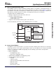
All pin multiplexing options are configurable by software via pin mux registers that reside in the System
Control Module. The PinMux0 Register controls the Video In muxing, PinMux1 register controls Video Out
signals, PinMux2 register controls AEMIF signals, PinMux3 registers control the multiplexing of the GIO
signals, the PinMux4 register controls the SPI and MMC/SD0 signals. Refer to the ARM Subsystem User's
Guide for complete descriptions of the pin mux registers.
There are five types of reset in DM355. The types of reset differ by how they are initiated and/or by their
effect on the chip. Each type is briefly described in Table 3-14 and further described in the ARM
Subsystem Guide.
Table 3-14. Reset Types
Type Initiator Effect
POR (Power-On-Reset) RESET pin low and TRST low Total reset of the chip (cold reset). Resets all modules
including memory and emulation.
Warm Reset RESET pin low and TRST high (initiated by ARM Resets all modules including memory, except ARM
emulator). emulation.
Max Reset ARM emulator or Watchdog Timer (WDT). Same effect as warm reset.
System Reset ARM emulator Resets all modules except memory and ARM
emulation. It is a soft reset that maintains memory
contents and does not affect or reset clocks or power
states.
Submit Documentation Feedback Detailed Device Description 79