
Digital Media System-on-Chip (DMSoC) Product Preview

www.ti.com
PRODUCT PREVIEW
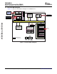
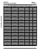
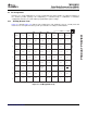
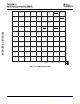
2.3 Pin Assignments
2.3.1 Pin Map (Bottom View)
9
J
8
V
SSA_PLL2
7
V
DDA33_USB
6
5
4
31
H
G
V
DDA13_USB
V
SS
F
E
D
CIN2
C
B
A
VREF
CIN3CIN0
V
DDA_PLL2
V
SS
LCD_OE
FIELDVCLK
V
SS
V
SS
CV
DD
VSYNCEXTCLKVFB
V
DD_VOUT
V
DD_VOUT
V
DD_VOUT
HSYNCCOUT0COUT1TVOUT
TDOEMU0EMU1
V
SS_USB
USB_VBUS
COUT2COUT3IOUT
TDITMS
V
SS_USB
USB_IDCOUT4
V
SS
TRST
V
SS_USB_REF
USB_R1
V
DDD13_USB
USB_DRV
VBUS
CV
DD
YOUT7COUT5
MXO1
V
SS
V
SS_USB
V
DDA33_USB_
PLL
V
SS
YOUT5YOUT4YOUT0
MXI1
V
SS
USB_DPUSB_DM
V
SS
YOUT6YOUT2
CV
DD
2
V
SS
V
SS
V
SS
IBIAS
V
SS
COUT6
COUT7
YOUT3
YOUT1
RSV01
V
DD
V
DD
NC
TMS320DM355
Digital Media System-on-Chip (DMSoC)
SPRS463A – SEPTEMBER 2007 – REVISED SEPTEMBER 2007
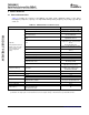
Extensive use of pin multiplexing is used to accommodate the largest number of peripheral functions in
the smallest possible package. Pin multiplexing is controlled using a combination of hardware
configuration at device reset and software programmable register settings.
Figure 2-1 through Figure 2-4 show the pin assignments in four quadrants (A, B, C, and D). Note that
micro-vias are not required. Contact your TI representative for routing recommendations.
Figure 2-1. Pin Map [Quadrant A]
Submit Documentation Feedback Device Overview 9