
Digital Media System-on-Chip (DMSoC) Product Preview

www.ti.com
PRODUCT PREVIEW
5 Peripheral Information and Electrical Specifications
5.1 Parameter Information Device-Specific Information
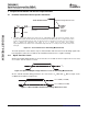
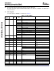
TransmissionLine
4.0pF 1.85pF
Z0=50 Ω
(seenote)
Tester PinElectronics
Data SheetTimingReferencePoint
Output
Under
Test
42 Ω 3.5nH
DevicePin
(seenote)
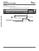
5.1.1 Signal Transition Levels
V
ref
V
ref
=V
IL
MAX(orV
OL
MAX)
V
ref
=V
IH
MIN(orV
OH
MIN)
TMS320DM355
Digital Media System-on-Chip (DMSoC)
SPRS463A – SEPTEMBER 2007 – REVISED SEPTEMBER 2007
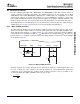
A. The data sheet provides timing at the device pin. For output timing analysis, the tester pin electronics and its
transmission line effects must be taken into account. A transmission line with a delay of 2 ns or longer can be used to
produce the desired transmission line effect. The transmission line is intended as a load only. It is not necessary to
add or subtract the transmission line delay (2 ns or longer) from the data sheet timings.
Input requirements in this data sheet are tested with an input slew rate of < 4 Volts per nanosecond (4 V/ns) at the
device pin.
Figure 5-1. Test Load Circuit for AC Timing Measurements
The load capacitance value stated is only for characterization and measurement of AC timing signals. This
load capacitance value does not indicate the maximum load the device is capable of driving.
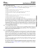
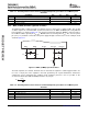
All input and output timing parameters are referenced to V
ref
for both "0" and "1" logic levels. For 3.3 V I/O,
V
ref
= 1.65 V. For 1.8 V I/O, V
ref
= 0.9 V.
Figure 5-2. Input and Output Voltage Reference Levels for AC Timing Measurements
All rise and fall transition timing parameters are referenced to V
IL
MAX and V
IH
MIN for input clocks,
V
OL
MAX and V
OH
MIN for output clocks.
Figure 5-3. Rise and Fall Transition Time Voltage Reference Levels
94 Peripheral Information and Electrical Specifications Submit Documentation Feedback