
Digital Media System-on-Chip (DMSoC) Product Preview

www.ti.com
PRODUCT PREVIEW
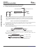
5.2 Recommended Clock and Control Signal Transition Behavior
5.3 Power Supplies
TMS320DM355
Digital Media System-on-Chip (DMSoC)
SPRS463A – SEPTEMBER 2007 – REVISED SEPTEMBER 2007
All clocks and control signals should transition between V
IH
and V
IL
(or between V
IL
and V
IH
) in a
monotonic manner.
The power supplies of DM355 are summarized in Table 5-1 .
Table 5-1. Power Supplies
Customer Tolerance Package Chip Plane Description Comments
Board Plane Name
Supply
1.3 V ± 5% 1.3 V CV
DD
Core V
DD
V
DDA_PLL1
PLL1 V
DDA
V
DDA_PLL2
PLL2 V
DDA
V
DDD13_USB
USB 1.3 V supply
V
DDA13_USB
USB 1.3 V supply
3.3 V ± 5% 3.3 V V
DD
IO V
DD
for LVCMOS V
DDSHV
V
DD
IO V
DD
for MXI/O1 V
DDSHV
V
DD
IO V
DD
for MXI/O2 V
DDSHV1
V
DD
IO V
DD
for ISB DRVVBUS V
DDSHV2
V
DDA33_DDRDLL
DDR DLL analog V
DD
V
DDA33_USB
Analog 3.3 V power USB PHY
V
DDA33_USB_PLL
Common mode 3.3 V power for USB
PHY (PLL)
V
DD
IO V
DD
for peripherals
3.3 V ± 5% 3.3 V V
DD_VIN
IO V
DD
for VideoIN I/F
V
DD_VOUT
IO V
DD
for VideoOUT I/F
1.8 V ± 5% 1.8 V V
DD_DDR
1.8 V ± 5% 1.8 V V
DDA18
Analog 1.8 V power
1.8 V ± 5% 1.8 V V
DDA18_DAC
Place decoupling caps (0.1 μ F/10 μ f) close
to chip
0 V n/a 0 V V
SS_MX1
Connect to external crystal capacitor
ground
0 V n/a 0 V V
SS_MX2
Connect to external crystal capacitor
ground
0 V n/a 0 V V
SS
Chip ground
USB ESD ground
ground V
SS
0 V n/a 0 V V
SSA
ground Keep separate from digital ground V
SS
0 V n/a 0 V V
SA_PLL1
PLL1 V
SSA
0 V n/a 0 V V
SSA_PLL2
PLL2 V
SSA
0 V n/a 0 V V
SSA_DLL
DLL ground
0 V n/a 0 V V
SS_USB
USB ground V
SSA13_USB
V
SSA13_USB
V
SSA33_USB
V
SSA33_USB_PLL
0 V n/a 0 V V
SS_USB_REF
USB PHY reference ground V
SSREF
0 V n/a 0 V V
SSA_DAC
DAC ground Keep separate from digital ground V
SS
V
DDS
*0.5 V
DDS
*0.5 V
REFSSTL
DRR ref voltage V
DDS
divided by 2, through board resistors
5 V 5 V USB_VBUS VBUS Connect to external charge pump
Peripheral Information and Electrical Specifications96 Submit Documentation Feedback