TMS320DM643x DMP DDR2 Memory Controller User's Guide Literature Number: SPRU986B November 2007
SPRU986B – November 2007 Submit Documentation Feedback
Contents Preface ............................................................................................................................... 6 1 Introduction................................................................................................................ 7 2 1.1 Purpose of the Peripheral ....................................................................................... 7 1.2 Features ................................................................................................
List of Figures 1 2 3 4 5 6 7 8 9 10 11 12 13 14 15 16 17 18 19 20 21 22 23 24 25 26 27 28 29 30 31 32 4 Data Paths to DDR2 Memory Controller .................................................................................. 8 DDR2 Memory Controller Clock Block Diagram ......................................................................... 9 DDR2 Memory Controller Signals ........................................................................................ 11 Refresh Command .........................
List of Tables 1 2 3 4 5 6 7 8 9 10 11 12 13 14 15 16 17 18 19 20 21 22 23 24 25 26 27 28 29 30 31 32 33 34 35 36 37 38 A-1 PLLC2 Configuration ....................................................................................................... DDR2 Memory Controller Signal Descriptions ......................................................................... DDR2 SDRAM Commands ...............................................................................................
Preface SPRU986B – November 2007 Read This First About This Manual This document describes the DDR2 memory controller in the TMS320DM643x Digital Media Processor (DMP). Notational Conventions This document uses the following conventions. • Hexadecimal numbers are shown with the suffix h. For example, the following number is 40 hexadecimal (decimal 64): 40h. • Registers in this document are shown in figures and described in tables.
User's Guide SPRU986B – November 2007 DDR2 Memory Controller 1 Introduction This document describes the DDR2 memory controller in the TMS320DM643x Digital Media Processor (DMP). 1.1 Purpose of the Peripheral The DDR2 memory controller is used to interface with JESD79D-2A standard compliant DDR2 SDRAM devices. Memories types such as DDR1 SDRAM, SDR SDRAM, SBSRAM, and asynchronous memories are not supported. The DDR2 memory controller is the major memory location for program and data storage. 1.
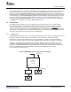
www.ti.com Introduction 1.3 Functional Block Diagram The DDR2 memory controller is the main interface to external DDR2 memory. Figure 1 displays the general data paths to on-chip peripherals and external DDR2 SDRAM. Master peripherals, EDMA, the ARM processor, and DSP can access the DDR2 memory controller through the switched central resource (SCR). Figure 1. Data Paths to DDR2 Memory Controller DSP Master peripherals SCR BUS EDMA DDR2 memory controller BUS External DDR2 SDRAM VPSS 1.
www.ti.com Peripheral Architecture 2 Peripheral Architecture This section describes the architecture of the DDR2 memory controller as well as how it is structured and how it works within the context of the system-on-a-chip. The DDR2 memory controller can gluelessly interface to most standard DDR2 SDRAM devices and supports such features as self-refresh mode and prioritized refresh.
www.ti.com Peripheral Architecture 2.1.2 Clock Configuration The frequency of PLL2_SYSCLK1 is configured by selecting the appropriate PLL multiplier and divider ratio. The PLL multiplier and divider ratio are selected by programming registers within PLLC2. Table 1 shows a list of PLL multiplier and divider settings to achieve certain DDR2 frequencies. The data in Table 1 is derived by assuming a 27-MHZ reference clock. See the device-specific data manual for the clock frequencies that are supported.
www.ti.com Peripheral Architecture 2.3 Signal Descriptions The DDR2 memory controller signals are shown in Figure 3 and described in Table 2. The following features are included: • • • • • The maximum data bus is 32-bits wide. The address bus is 13-bits wide with an additional 3 bank address pins. Two differential output clocks driven by internal clock sources. Command signals: Row and column address strobe, write enable strobe, data strobe, and data mask.
www.ti.com Peripheral Architecture 2.4 Protocol Description(s) The DDR2 memory controller supports the DDR2 SDRAM commands listed in Table 3. Table 4 shows the signal truth table for the DDR2 SDRAM commands. Table 3. DDR2 SDRAM Commands Command Function ACTV Activates the selected bank and row. DCAB Precharge all command. Deactivates (precharges) all banks. DEAC Precharge single command. Deactivates (precharges) a single bank. DESEL Device Deselect. EMRS Extended Mode Register set.
www.ti.com Peripheral Architecture 2.4.1 Refresh Mode The DDR2 memory controller issues refresh commands to the DDR2 SDRAM memory (Figure 4). REFR is automatically preceded by a DCAB command, ensuring the deactivation of all CE spaces and banks selected. Following the DCAB command, the DDR2 memory controller begins performing refreshes at a rate defined by the refresh rate (RR) bit in the SDRAM refresh control register (SDRCR).
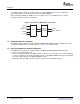
www.ti.com Peripheral Architecture 2.4.2 Deactivation (DCAB and DEAC) The precharge all banks command (DCAB) is performed after a reset to the DDR2 memory controller or following the initialization sequence. DDR2 SDRAMs also require this cycle prior to a refresh (REFR) and mode set register commands (MRS and EMRS). During a DCAB command, DDR_A[10] is driven high to ensure the deactivation of all banks. Figure 5 shows the timing diagram for a DCAB command. Figure 5.
www.ti.com Peripheral Architecture The DEAC command closes a single bank of memory specified by the bank select signals. Figure 6 shows the timings diagram for a DEAC command. Figure 6.
www.ti.com Peripheral Architecture 2.4.3 Activation (ACTV) The DDR2 memory controller automatically issues the activate (ACTV) command before a read or write to a closed row of memory. The ACTV command opens a row of memory, allowing future accesses (reads or writes) with minimum latency. The value of DDR_BA[2:0] selects the bank and the value of A[12:0] selects the row. When the DDR2 memory controller issues an ACTV command, a delay of tRCD is incurred before a read or write command is issued.
www.ti.com Peripheral Architecture 2.4.4 READ Command Figure 8 shows the DDR2 memory controller performing a read burst from DDR2 SDRAM. The READ command initiates a burst read operation to an active row. During the READ command, DDR_CAS drives low, DDR_WE and DDR_RAS remain high, the column address is driven on DDR_A[12:0], and the bank address is driven on DDR_BA[2:0]. The DDR2 memory controller uses a burst length of 8, and has a programmable CAS latency of 2, 3, 4, or 5.
www.ti.com Peripheral Architecture 2.4.5 Write (WRT) Command Prior to a WRT command, the desired bank and row are activated by the ACTV command. Following the WRT command, a write latency is incurred. Write latency is equal to CAS latency minus 1. All writes have a burst length of 8. The use of the DDR_DQM outputs allows byte and halfword writes to be executed. Figure 9 shows the timing for a write on the DDR2 memory controller.
www.ti.com Peripheral Architecture 2.4.6 Mode Register Set (MRS and EMRS) DDR2 SDRAM contains mode and extended mode registers that configure the DDR2 memory for operation. These registers control burst type, burst length, CAS latency, DLL enable/disable (on DDR2 device), single-ended strobe, etc. The DDR2 memory controller programs the mode and extended mode registers of the DDR2 memory by issuing MRS and EMRS commands.
www.ti.com Peripheral Architecture 2.5 Memory Width and Byte Alignment The DDR2 memory controller supports memory widths of 16 bits and 32 bits. Table 5 summarizes the addressable memory ranges on the DDR2 memory controller. See the device-specific data manual for the memory widths that are supported. Figure 11 shows the byte lanes used on the DDR2 memory controller. The external memory is always right-aligned on the data bus. Table 5.
www.ti.com Peripheral Architecture 2.6 Endianness Considerations The DDR2 memory controller supports little-endian operating mode. This determines the order in which data on the internal data bus is written to or read from devices that are not as wide as the internal data bus. However, the DDR2 memory controller maintains the natural order of endian operations. That is, a stream of data starting at any address N will always be accessed in the correct or incrementing data order.
www.ti.com Peripheral Architecture 2.7 Address Mapping The DDR2 memory controller views external DDR2 SDRAM as one continuous block of memory. This statement is true regardless of the number of external physical devices mapped to a given chip select space. The DDR2 memory controller receives DDR2 memory access requests along with a 32-bit logical address from the rest of the system.
www.ti.com Peripheral Architecture Table 9.
www.ti.com Peripheral Architecture Figure 12. Logical Address-to-DDR2 SDRAM Address Map Col. 0 Col. 1 Col. 2 Col. 3 Col. 4 Col. M−1 Col.
www.ti.com Peripheral Architecture Figure 13.
www.ti.com Peripheral Architecture 2.8 DDR2 Memory Controller Interface To move data efficiently from on-chip resources to external DDR2 SDRAM memory, the DDR2 memory controller makes use of a command FIFO, a write FIFO, a read FIFO, and command and data schedulers. Table 11 describes the purpose of each FIFO. Figure 14 shows the block diagram of the DDR2 memory controller FIFOs. Commands, write data, and read data arrive at the DDR2 memory controller parallel to each other.
www.ti.com Peripheral Architecture 2.8.1 Command Ordering and Scheduling, Advanced Concept The DDR2 memory controller performs command re-ordering and scheduling in an attempt to achieve efficient transfers with maximum throughput. The goal is to maximize the utilization of the data, address, and command buses while hiding the overhead of opening and closing DDR2 SDRAM rows. Command re-ordering takes place within the command FIFO. Typically, a given master issues commands on a single priority.
www.ti.com Peripheral Architecture 2.8.2 Command Starvation The reordering and scheduling rules listed above may lead to command starvation, which is the prevention of certain commands from being processed by the DDR2 memory controller.
www.ti.com Peripheral Architecture 2.9 Refresh Scheduling The DDR2 memory controller issues autorefresh (REFR) commands to DDR2 SDRAM devices at a rate defined in the refresh rate (RR) bit field in the SDRAM refresh control register (SDRCR). A refresh interval counter is loaded with the value of the RR bit field and decrements by 1 each cycle until it reaches zero. Once the interval counter reaches zero, it reloads with the value of the RR bit.
www.ti.com Peripheral Architecture Once in self-refresh mode, the DDR2 memory controller input clocks (VCLK and X2_CLK) may be gated off or changed in frequency. Stable clocks must be present before exiting self-refresh mode. See Section 2.16 for more information describing the proper procedure to follow when shutting down DDR2 memory controller input clocks. 2.11 Reset Considerations The DDR2 memory controller has two reset signals, VRST and VCTL_RST.
www.ti.com Peripheral Architecture 2.12 VTP IO Buffer Calibration The DDR2 memory controller is able to control the impedance of the output IO. This feature allows the DDR2 memory controller to tune the output impedance of the IO to match that of the PCB board. Control of the output impedance of the IO is an important feature because impedance matching reduces reflections, creating a cleaner board design.
www.ti.com Peripheral Architecture Table 14. DDR2 SDRAM Configuration by MRS Command DDR2 Memory Controller Address Bus Value DDR2 SDRAM Register Bit DDR2 SDRAM Field Function Selection DDR_A[12] 0 12 Power Down Exit Fast exit DDR_A[11:9] t_WR 11:9 Write Recovery Write recovery from autoprecharge. Value of 2, 3, 4, 5, or 6 is programmed based on value of the T_WR bit in the SDRAM timing register (SDTIMR).
www.ti.com Peripheral Architecture 2.13.2 Initializing Following Device Power Up and Device RESET CAUTION The following power-up sequence is preliminary and is documented to reflect the intended-use case. This power-up sequence may change at a future date. Following device power up, the DDR2 memory controller is held in reset with the internal clocks to the module gated off. Before releasing the DDR2 memory controller from reset, the clocks to the module must be turned on.
www.ti.com Peripheral Architecture 2.14 Interrupt Support The DDR2 memory controller supports two addressing modes, linear incrementing and cache line wrap. Upon receipt of an access request for an unsupported addressing mode, the DDR2 memory controller generates an interrupt by setting the LT bit in the interrupt raw register (IRR). The DDR2 memory controller will then treat the request as a linear incrementing request.
www.ti.com Peripheral Architecture 2.16.1 DDR2 Memory Controller Clock Stop Procedure CAUTION The following clock stop procedures are preliminary and are documented to reflect the intended-use cases. These clock stop procedures may change at a future date. Note: If an access occurs to the DDR2 memory controller after completing steps 1-5, the DLL will wake up and lock, then the MCLK will turn on and the access will be performed.
www.ti.com Supported Use Cases 3 Supported Use Cases The DDR2 memory controller allows a high degree of programmability for shaping DDR2 accesses. The programmability inherent to the DDR2 memory controller provides the DDR2 memory controller with the flexibility to interface with a variety of DDR2 devices.
www.ti.com Supported Use Cases Figure 17.
www.ti.com Supported Use Cases 3.2.1 Configuring SDRAM Bank Configuration Register (SDBCR) The SDRAM bank configuration register (SDBCR) contains register fields that configure the DDR2 memory controller to match the data bus width, CAS latency, number of banks, and page size of the attached DDR2 memory. In this example, we assume the following configuration: • Data bus width = 32 bits • CAS latency = 4 • Number of banks = 8 • Page size = 1024 words Table 16 shows the resulting SDBCR configuration.
www.ti.com Supported Use Cases 3.2.3 Configuring SDRAM Timing Registers (SDTIMR and SDTIMR2) The SDRAM timing register (SDTIMR) and SDRAM timing register 2 (SDTIMR2) configure the DDR2 memory controller to meet the data sheet timing parameters of the attached DDR2 device. Each field in SDTIMR and SDTIMR2 corresponds to a timing parameter in the DDR2 data sheet specification.
www.ti.com DDR2 Memory Controller Registers 3.2.4 Configuring DDR PHY Control Register (DDRPHYCR) The DDR PHY control register (DDRPHYCR) contains a read latency (READLAT) field that helps the DDR2 memory controller determine when to sample read data. The READLAT field should be programmed to a value equal to CAS latency plus round trip board delay minus 1.
www.ti.com DDR2 Memory Controller Registers Table 22. DDR2 Memory Controller Registers Relative to Base Address 2000 0000h Offset Acronym Register Description Section 4h SDRSTAT SDRAM Status Register Section 4.1 8h SDBCR SDRAM Bank Configuration Register Section 4.2 Ch SDRCR SDRAM Refresh Control Register Section 4.3 10h SDTIMR SDRAM Timing Register Section 4.4 14h SDTIMR2 SDRAM Timing Register 2 Section 4.5 20h PBBPR Peripheral Bus Burst Priority Register Section 4.
www.ti.com DDR2 Memory Controller Registers 4.2 SDRAM Bank Configuration Register (SDBCR) The SDRAM bank configuration register (SDBCR) contains fields that program the DDR2 memory controller to meet the specification of the attached DDR2 memory. These fields configure the DDR2 memory controller to match the data bus width, CAS latency, number of internal banks, and page size of the attached DDR2 memory. The SDBCR is shown in Figure 20 and described in Table 26.
www.ti.com DDR2 Memory Controller Registers Table 26. SDRAM Bank Configuration Register (SDBCR) Field Descriptions (continued) Bit 11-9 Field CL 8-7 Reserved 6-4 IBANK Value Description 0-7h CAS latency. 0-1h Reserved 2h CAS latency of 2 3h CAS latency of 3 4h CAS latency of 4 5h CAS latency of 5 6h-7h Reserved 0 Reserved 0-7h 0 1 bank 1h 2 banks 2h 4 banks 3h 8 banks 4h-7h 3 2-0 Reserved PAGESIZE 0 0-7h Reserved Reserved. Always write a 0 to this bit. DDR2 page size.
www.ti.com DDR2 Memory Controller Registers 4.3 SDRAM Refresh Control Register (SDRCR) The SDRAM refresh control register (SDRCR) is used to configure the DDR2 memory controller to: • Enter and Exit the self-refresh state. • Enable and disable MCLK, stopping when in the self-refresh state. • Meet the refresh requirement of the attached DDR2 device by programming the rate at which the DDR2 memory controller issues autorefresh commands. The SDRCR is shown in Figure 21 and described in Table 27. Figure 21.
www.ti.com DDR2 Memory Controller Registers 4.4 SDRAM Timing Register (SDTIMR) The SDRAM timing register (SDTIMR) configures the DDR2 memory controller to meet many of the AC timing specification of the DDR2 memory. The SDTIMR register is programmable only when the TIMUNLOCK bit is set to 1 in the SDBCR. Note that DDR_CLK is equal to the period of the DDR_CLK signal. See the DDR2 memory data sheet for information on the appropriate values to program each field.
www.ti.com DDR2 Memory Controller Registers 4.5 SDRAM Timing Register 2 (SDTIMR2) Like the SDRAM timing register (SDTIMR), the SDRAM timing register 2 (SDTIMR2) also configures the DDR2 memory controller to meet the AC timing specification of the DDR2 memory. The SDTIMR2 register is programmable only when the TIMUNLOCK bit is set to 1 in the SDBCR. See the DDR2 data sheet for information on the appropriate values to program each field. SDTIMR2 is shown in Figure 23 and described in Table 29. Figure 23.
www.ti.com DDR2 Memory Controller Registers 4.6 Peripheral Bus Burst Priority Register (PBBPR) The peripheral bus burst priority register (PBBPR) helps prevent command starvation within the DDR2 memory controller. To avoid command starvation, the DDR2 memory controller momentarily raises the priority of the oldest command in the command FIFO after a set number of transfers have been made.
www.ti.com DDR2 Memory Controller Registers 4.7 Interrupt Raw Register (IRR) The interrupt raw register (IRR) displays the raw status of the interrupt. If the interrupt condition occurs, the corresponding bit in IRR is set independent of whether or not the interrupt is enabled. The IRR is shown in Figure 25 and described in Table 31. Figure 25.
www.ti.com DDR2 Memory Controller Registers 4.8 Interrupt Masked Register (IMR) The interrupt masked register (IMR) displays the status of the interrupt when it is enabled. If the interrupt condition occurs and the corresponding bit in the interrupt mask set register (IMSR) is set, then the IMR bit is set. The IMR bit is not set if the interrupt is not enabled in IMSR. The IMR is shown in Figure 26 and described in Table 32. Figure 26.
www.ti.com DDR2 Memory Controller Registers 4.9 Interrupt Mask Set Register (IMSR) The interrupt mask set register (IMSR) enables the DDR2 memory controller interrupt. The IMSR is shown in Figure 27 and described in Table 33. Note: If the LTMSET bit in IMSR is set concurrently with the LTMCLR bit in the interrupt mask clear register (IMCR), the interrupt is not enabled and neither bit is set to 1. Figure 27.
www.ti.com DDR2 Memory Controller Registers 4.10 Interrupt Mask Clear Register (IMCR) The interrupt mask clear register (IMCR) disables the DDR2 memory controller interrupt. Once an interrupt is enabled, it may be disabled by writing a 1 to the IMCR bit. The IMCR is shown in Figure 28 and described in Table 34. Note: If the LTMCLR bit in IMCR is set concurrently with the LTMSET bit in the interrupt mask set register (IMSR), the interrupt is not enabled and neither bit is set to 1. Figure 28.
www.ti.com DDR2 Memory Controller Registers 4.11 DDR PHY Control Register (DDRPHYCR) The DDR PHY control register (DDRPHYCR) configures the DDR2 memory controller DLL for operation and determines whether the DLL is in reset, whether it is powered up, and the read latency. The DDRPHYCR is shown in Figure 29 and described in Table 35. Figure 29.
www.ti.com DDR2 Memory Controller Registers 4.12 VTP IO Control Register (VTPIOCR) The VTP IO control register (VTPIOCR) is used to control the calibration of the DDR2 memory controller IOs with respect to voltage, temperature, and process (VTP). The voltage, temperature, and process information is used to control the IO's output impedance. The VTPIOCR is shown in Figure 30 and described in Table 36. Figure 30.
www.ti.com DDR2 Memory Controller Registers 4.13 DDR VTP Register (DDRVTPR) The DDR VTP register (DDRVTPR) is used in conjunction with the VTP IO control register (VTPIOCR) to calibrate the output impedance of the DDR2 memory controller IOs with respect to voltage, temperature, and process. Following the calibration sequence, DDRVTPR contains the information needed to calibrate the impedance of the IO.
www.ti.com Appendix A Appendix A Revision History Table A-1 lists the changes made since the previous version of this document. Table A-1. Document Revision History Reference Additions/Modifications/Deletions Global Changed DDR_CLKO to DDR_CLK in text, figures, and tables. Global Changed DDR_CLKO to DDR_CLK in text, figures, and tables. Global Changed DDR_BS[2:0] to DDR_BA[2:0] in text, figures, and tables. Section 2.1 Changed paragraph. Section 2.1.1 Changed subsection.
IMPORTANT NOTICE Texas Instruments Incorporated and its subsidiaries (TI) reserve the right to make corrections, modifications, enhancements, improvements, and other changes to its products and services at any time and to discontinue any product or service without notice. Customers should obtain the latest relevant information before placing orders and should verify that such information is current and complete.