
Computer Hardware User Manual

Architecture
www.ti.com
2.5.6.4 NAND Read and Program Operations
A NAND Flash access cycle is composed of a command, address, and data phase. The EMIF will not
automatically generate these three phases to complete a NAND access with one transfer request. To
complete a NAND access cycle, multiple single asynchronous access cycles (as described above) must
be completed by the EMIF. Software must be used to request the appropriate asynchronous accesses to
complete a NAND Flash access cycle. This software must be developed to the specification of the chosen
NAND Flash device.
Since NAND operations are divided into single asynchronous access cycles, the chip select signal will not
remain activated for the duration of the NAND operation. Instead, the chip select signal will deactivate
between each asynchronous access cycle. For this reason, the EMIF does not support NAND Flash
devices that require the chip select signal to remain low during the t
R
time for a read. See Section 2.5.6.8
for workaround.
Care must be taken when performing a NAND read or write operation via the EDMA. See Section 2.5.6.5
for more details.
NOTE: The EMIF does not support NAND Flash devices that require the chip select signal to
remain low during the t
R
time for a read. See Section 2.5.6.8 for workaround.
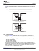
2.5.6.5 NAND Data Read and Write via DMA
When performing NAND accesses, the EDMA is most efficiently used for the data phase of the access.
The command and address phases of the NAND access require only a few words of data to be
transferred and therefore do not take advantage of the EDMA's ability to transfer larger quantities of data
with a single request. In this section we will focus on using the EDMA for the data phase of a NAND
access.
There are two conditions that require care to be taken when performing NAND reads and writes via the
EDMA. These are:
• CLE_EM_A[2] and ALE_EM_A[1] are lower address lines and must be driven low
• The EMIF does not support a constant address mode, but only supports linear incrementing address
modes.
Since the EMIF does not support a constant addressing mode, when programming the EDMA, a linear
incrementing address mode must be used. When using a linear incrementing address mode, since the
CLE and ALE are driven by lower address lines, care must be taken not to increase the address into a
range the drives CLE and/or ALE high. To prevent the address from incrementing into a range that drives
CLE and/or ALE high, the EDMA ACNT, BCNT, SIDX, DIDX, and synchronization type must be
programmed appropriately. The proper EDMA configurations are described below.
EDMA setup for a NAND Flash data read:
• ACNT ≤ 8 bytes (this can also be set to less than or equal to the external data bus width)
• BCNT = transfer size in bytes/ACNT
• SIDX (source index) = 0
• DIDX (destination index) = ACNT
• AB synchronized
EDMA setup for a NAND Flash data write:
• ACNT ≤ 8 bytes (this can also be set to less than or equal to the external data bus width)
• BCNT = transfer size in bytes/ACNT
• SIDX (source index) = ACNT
• DIDX (destination index) = 0
• AB synchronized
24
Asynchronous External Memory Interface (EMIF) SPRUEQ7C–February 2010
Submit Documentation Feedback
Copyright © 2010, Texas Instruments Incorporated