
Computer Hardware User Manual
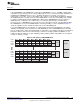

EM_D[15:0]
EM_RW
EM_A[1:0]
EM_WAIT
EM_OE
EM_WE
EM_CS
EM_BA1
GPIOx
AEMIF
HD[15:0]
HR/W
HCNTL[1:0]
HRDY
HDS1
HCS
HHWIL
HINT
HDS2
HAS
HPIENA
HBED
A
HBE1
A
HPI16
VCC
VCC
VSS
VSS
Architecture
www.ti.com
2.5.6.7 NAND Flash Status Register (NANDFSR)
The NAND Flash status register (NANDFSR) indicates the raw status of the EM_WAITn pin. The
EM_WAITn pin should be connected to the NAND Flash device's R/B signal, so that it indicates whether
or not the NAND Flash device is busy. During a read, the R/B signal will transition and remain low while
the NAND Flash retrieves the data requested. Once the R/B signal transitions high, the requested data is
ready and should be read by the EMIF. During a write/program operation, the R/B signal transitions and
remains low while the NAND Flash is programming the Flash with the data it has received from the EMIF.
Once the R/B signal transitions high, the data has been written to the Flash and the next phase of the
transaction may be performed. From this explanation, you can see that the NAND Flash status register is
useful to the software for indicating the status of the NAND Flash device and determining when to proceed
to the next phase of a NAND Flash operation.
When a rising edge occurs on the EM_WAITn pin, the EMIF sets the WR (wait rise) bit in the EMIF
interrupt raw register (EIRR). Therefore, the EMIF wait rise interrupt may be used to indicate the status of
the NAND Flash device. The WPn bit in the asynchronous wait cycle configuration register (AWCCR)
does not affect the NAND Flash status register (NANDFSR) or the WRn bit in EIRR. See Section 2.5.11.1
for more a detailed description of the wait rise interrupt.
2.5.6.8 Interfacing to a Non-CE Don't Care NAND Flash
As explained in Section 2.5.6.4, the EMIF does not support NAND Flash devices that require the chip
select signal to remain low during the t
R
time for a read. One way to work around this limitation is to use a
GPIO pin to drive the CE signal of the NAND Flash device. If this work around is implemented, software
will configure the selected GPIO to be low, then begin the NAND Flash operation, starting with the
command phase. Once the NAND Flash operation has completed the software will configure the selected
GPIO to be high. See Section 3 for more details on the GPIO workaround.
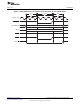
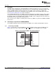
2.5.7 Interfacing to a TI DSP HPI
The EMIF supports connecting as a host to a TI DSP HPI interface. When connecting to a TI DSP HPI
interface, the EMIF must be configured for normal mode operation. Figure 10 shows the connection
diagram.
Figure 10. EMIF to 16-Bit Multiplexed HPI16 Interface
A HBE signals may not be present on all HPI interfaces.
26
Asynchronous External Memory Interface (EMIF) SPRUEQ7C–February 2010
Submit Documentation Feedback
Copyright © 2010, Texas Instruments Incorporated