
Computer Hardware User Manual
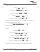
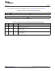

W_SETUP w max
ǒ
t
CLS
(m)
t
cyc
,
t
ALS
(m)
t
cyc
,
t
CS
(m)
t
cyc
Ǔ
* 1
W_STROBE w
t
WP
(m)
t
cyc
* 1
W_SETUP ) W_STROBE w
t
DS
(m)
t
cyc
* 1
W_HOLD w max
ǒ
t
CLH
(m)
t
cyc
,
t
ALH
(m)
t
cyc
,
t
CH
(m)
t
cyc
,
t
DH
(m)
t
cyc
Ǔ
* 1
W_SETUP ) W_STROBE ) W_HOLD w
t
WC
(m)
t
cyc
* 3
Use Cases
www.ti.com
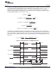
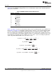
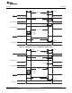
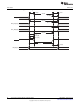
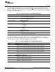
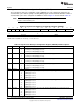
To determine the required EMIF configuration to interface to the NAND Flash for a write operation,
Table 27 lists the NAND AC timing parameters for a command latch, address latch, and data input latch
that must be considered.
Table 27. NAND Flash Write Timing Requirements
Parameter Description
t
WP
Write Pulse width
t
CLS
CLE Setup time
t
ALS
ALE Setup time
t
CS
CS Setup time
t
DS
Data Setup time
t
CLH
CLE Hold time
t
ALH
ALE Hold time
t
CH
CS Hold time
t
DH
Data Hold time
t
WC
Write Cycle time
Figure 17 to Figure 19 show the command latch, address latch, and data input latch of the NAND access.
From Figure 17 to Figure 19, the following equations may be derived. t
cyc
is the period at which the EMIF
operates. The W_SETUP, W_STROBE, and W_HOLD fields are programmed in terms of EMIF cycles
where as the data sheet specifications are typically given is nano seconds. This is explains the presence
of t
cyc
in the denominator of the following equations. A minus 1 is included in the equations because each
field in ACFGn is programmed in terms of EMIF clock cycles, minus 1 cycle. For example, W_SETUP is
equal to W_SETUP width in EMIF clock cycles minus 1 cycle.
42
Asynchronous External Memory Interface (EMIF) SPRUEQ7C–February 2010
Submit Documentation Feedback
Copyright © 2010, Texas Instruments Incorporated